InGaAs is one of the new wunderkind semiconductors, favored for high-electron-mobility transistors (HEMTs) and for optical designs (more about that in a future post). But, as with other more exotic materials, it isn’t silicon, and therefore it doesn’t benefit from silicon’s economics.
The problem is the lattice: to grow single-crystal stress-free InGaAs, you have to use a substrate with a similar lattice (you have some flexibility by adjusting the quantity of indium, which tweaks the lattice). Three III/V substrates available are GaAs, InAs, and InP, the latter of which is more typical. None of them is silicon.
Let’s say you want a semiconductor-over-insulator configuration using InGaAs instead of silicon (InGaAs-oI instead of SoI). You want a thin layer of pure InGaAs with an abrupt stop at the oxide. How are you going to do that?
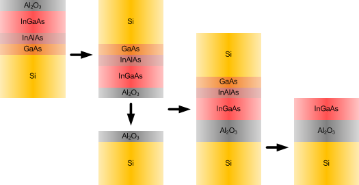
A team from the University of Tokyo, JST-CREST, and IntelliEPI came up with a wafer-bonding approach that uses only silicon substrates. The main difference from a traditional SoI wafer (well, aside from the InGaAs) is that the buried oxide (BOX) isn’t SiO2; it’s Al2O3.
The approach starts with the “donor” wafer, growing inGaAs on silicon. But… you can’t do that directly because of the lattice issue. So they laid down a couple “buffer” layers instead to ease between the lattices and keep the stresses low enough to allow single-crystal InGaAs to grow: GaAs, followed by InAlAs, topped with a layer of InGaAs.
A layer of oxide – Al2O3 – was then laid over the top. Yeah, you’ve pretty much got a bunch of layers of every combination of indium, gallium, arsenic, and aluminum in there.
Meanwhile, over on another silicon wafer, another layer of Al2O3 is laid down. The two oxide tops are polished, and then they are mated face-to-face. And all of the layers of the donor wafer except the InGaAs are etched away. What you’re left with is a top layer of InGaAs ending abruptly at the BOX edge. No mamby-pamby buffer layers left.
Electron mobility in the resulting layer was 1700 cm2/V, indicating low defectivity and high quality.
Note that the economics here come not just from the silicon material per se, but also from the fact that this provides a scaling path to 300-mm wafers, which aren’t available for more exotic substrates.
You can find their report (behind a paywall) here.
A separate team from UC San Diego, Nanyang Technological University in Singapore, and Los Alamos Labs also did some InGaAs work to deal with effective wafer flipping and bonding, published earlier this year. They used NiSi to effect the bonding. Their BOX layer was SiO2 (with a thin HfO2 buffer to the InGaAs layer). But, critically, the donor wafer was InP, not silicon.
You can find that full report here.