


It’s coming to a piece of silicon near you.
You may not create it; you may remain microns away from it. But there’s a good chance that, someday, it will be on your chip. And you might want to know something about it, because it will be your neighbor.
Exactly who is moving into your ‘hood? Just a few bizarre-looking circuits. Ones that look nothing like the circuits you’re used to. At all.
That’s because they don’t conduct electricity; they conduct light. We’re talking silicon photonics* here. And there’s been talk about it for a while, but, I don’t know, it feels to me like we’re starting to near the time when this becomes a reality for commercial chips. Call it a hunch.
My senses were first jarred when I saw some of the components used in a photonic circuit. They. Made. No. Sense. Whatsoever. So I’ve been doing some poking around, trying to figure stuff out based on the rather extensive amount of research on the web.
But it becomes clear very quickly that this is another of those fields (pun intended) that is 99% math. There’s plenty of intuitive stuff going on, but most folks stay firmly rooted in Maxwell’s equations, where divs and curls torment me as if in a stress dream. Those equations are important if you’re trying to create a circuit, but, since this is a photonics appreciation session rather than a design session, I’d like to keep us on a more intuitive level. (And, unlike quantum, intuition can have a role here.)
So… let’s start really basic. What we’re talking about here is the ability to integrate optical components into semiconductors. And, if everyone plays their cards right, the goal is silicon photonics so that we get the economics of high-volume silicon. And so that we can integrate electronics and optics together on the same chip.
Let’s get one thing out of the way first: while, as we’ll see, silicon has some nice properties for optics, the one thing it’s not good at is generating the light that will course its way around a chip. With its indirect bandgap, it needs the help of phonons to get the excitement right. While we try to solve that puzzle in the long term, we use other materials for lasing – which means either multi-chip or complex heterogeneous materials integration – mostly involving III/V-to-silicon wafer bonding, which limits the size of wafers (III/V materials don’t come in wafers as big as are available with silicon).
Either way, it’s a pain in the glass, something that hopeful scientists are trying to remedy. In fact, just this year, UCSB did some work creating quantum wells in silicon that can lase. But, here again, the silicon isn’t doing the lasing: they grew GaAs on silicon and then grew InAs quantum dots on that. So it’s still a mixed-materials game, but, in this case, one that leverages the full wafer size available in silicon.
So, for the rest of this, we’ll assume we have a suitable source of light. Now we need to do things like guide it, filter it, mix it, and unmix it. And filtering (or mixing) doesn’t mean only by frequency; it could also deal with specific modes or polarizations.
The first thing we need to do is to get the light from point A to point B. And silicon turns out to be really good at that. For light with wavelengths greater than 1.1 µm, it turns out that silicon is a lossless conductor. OK, an infinite-extent sheet of silicon is, anyway. There is loss from scattering at the rough boundaries, but not within the waveguide, where light travels by total internal reflection (TIF).
Also, if you take the waveguide and curve it, you’re going to get some losses. The tighter the curve, the greater the loss. And tight curves are better for tight integration, so this becomes a tradeoff.
There appear to be two main forms of waveguide: rib and strip. The main difference is that ribs are connected by silicon, while strips aren’t. Strips, due to the greater etching required, have more edge roughness and therefore greater loss. It would seem, however, that they can have tighter bends, which helps with compactness.
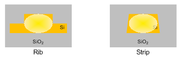
Figure 1. Cross sections of rib and strip waveguides.
The next concept we’ll discuss is key to making sense out of anything photonic: the evanescent field. Obviously light travels as an electromagnetic field, and the idea is to confine it within the waveguide. But the math doesn’t allow for the field to disappear discontinuously at the waveguide edge. So the field extends outside the waveguide and decays exponentially. That means that, for some distance away from the waveguide, you can “feel” the field inside the waveguide.

Figure 2. Conceptual view of evanescent field.
That distance away isn’t trivial. It can be farther than the width of the waveguide itself. Which means that, if you want to have two waveguides running next to each other, they need to be spaced far enough apart to where they don’t feel each other. Cross-talk isn’t just for electrical wires.
On the other hand, this becomes a useful feature for coupling the light from one waveguide into another.
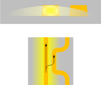
Figure 3. Using the evanescent field to couple light onto an adjacent line
(top: cross-section; bottom: top view).
Yes, you’re seeing that right. Simply by placing one waveguide next to another, the signal from one will show up on the other. This is a basic coupler. Obviously there are some energy conservation things going on here such that we’re not creating something out of nothing; that’s what lots of those equations are good for: deciding what power fraction, frequency, mode, and/or polarization hops across the barrier.
It has some other implications, but, before we get to those, we need to look at one other important component: the grating. You’ll often see the name “Bragg” accompanying this. Such gratings cause reflections and deflections; the spacing of the grating determines which frequencies are affected.
If you read last week’s piece about optical sensing of MEMS cantilevers, you might remember that gratings were placed under each cantilever to deflect light out and then reaccept it back in. That’s exactly what we’re talking about here.
The configuration of the grating also has an impact on its efficiency, since it deflects light both up and down. I’ve seen one option to put a mirror under the grating to reflect any downward light back up, but having the grating raised above the level of the surrounding silicon also appears to help.
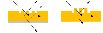
Figure 4. Gratings allow capture of light or the deflecting off of a portion of the light. On the left, the light splits up and down; an optional mirror could return the downward light. On the right, higher grating ribs send the light up preferentially.
Gratings are also used to accept light from an outside fiber into the chip. This isn’t needed if the light is coming in horizontally, but such a setup doesn’t allow for a photonic chip to be tested in wafer form (since the tester can’t access the edge of the chip). Instead, the light comes from above and is accepted into the waveguide by the grating. A separate grating sends the light off-chip in the same manner.
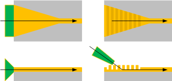
Figure 5. Simplified structures for getting light into the chip (top is top view; bottom is side view). The left version requries light coming in from the edge of the die (not possible before dicing the wafer); on the right, a grating brings in non-horizontal light. Similar structures are used for output.
The funnel shape is needed to take the light, which had been free to roam a relatively large fiber, and gently coax it into the much tighter confines of the on-chip waveguide.
These gratings also reflect (and they are used, conceptually, in the complex masks needed for extreme ultraviolet (EUV) lithography, which employs all reflective optics). Combine that with the splitting effect we saw above, and you can build an add-drop filter. The grating between the waveguides reflects the selected frequency, which effectively drops that frequency from the signal. You can also add a selective frequency.
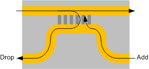
Figure 6. An add-drop filter built from a contra-directional coupler.
Because, in this case, the light in the waveguides travels in opposite directions (from the left on top; from the right on the bottom), this is called a “contra-directional” coupler. There are also co-directional couplers.
Finally, the coolest one of them all. This is the one I saw originally that clued me into the fact that I had a lot to learn here. A circle (or loop) forms a resonator. Some of the light from a waveguide gets coupled onto the resonator, and the diameter of the resonator reinforces a particular frequency. Simplistically speaking, the light travels around and around forever. But, of course, that can’t be – at the very least, the constant curving will dissipate some of the light. But as long as there is light in the feeding waveguide, it will keep topping up the resonator.
And, of course, if you never do anything with the light – if you just leave it in there – well, then it really does no good. How about peeling it off on the other side? By doing that, you’ve pulled a specific wavelength from the original guide, selecting it via the resonator, and then you’ve coupled that wavelength off onto a new waveguide.
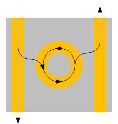
Figure 7. A resonator peeling off one wavelength and coupling it onto another waveguide.
What’s cooler yet is that you can chain these resonators together, doing a series of handoffs that might rival The Play.** What does this give you? Well, at the very least, an optical delay line. You can use that to create an interferometer, for example. Such a string of coupled resonators is called a coupled-resonator optical waveguide (CROW). Even though it’s made of separate pieces of waveguide, it does carry the light along in the manner of a waveguide, albeit more circuitously.
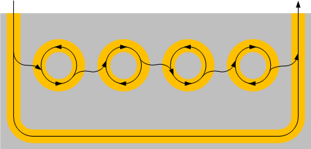
Figure 8. Coupled-resonator optical waveguide (CROW) used as a delay line to create an interferometer.
There’s lots more nuance and lots more variations, but I’m not going to delve that deeply. I’m already in a bit further than I deserve to be. I’ve probably already betrayed my ignorance too much; no sense risking a total unmasking.
But there is one other interesting concept coming: so-called photonic crystals. The idea here is to engineer a structure that looks like a lattice (in 1, 2, or 3 dimensions), only sized and spaced for photons. You then use irregularities to confine and guide the light.
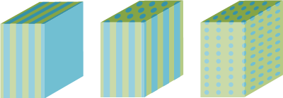
Figure 9. Conceptual view of photonic crystals: (left) 1D; (middle) 2D; and (right) 3D. 3D crystals are much more challenging to fabricate.
For example, the resonator of Figure 7 might look more like the following using a photonic crystal.
Figure 10. A resonator in a photonic crystal (top view).
So there you are. A quick-and-dirty look at some photonics basics. Now when that odd new neighbor moves in, you can greet it with cheerful familiarity. Be sure to bring some lasagna by to make it feel welcome.
Of course, this does leave one important matter untouched: How does one design this stuff? Are there tools for automating the work? Ah, well, that’s a topic for a couple of weeks from now.
*As a quick jargon tip, in case you want to go look some of this stuff up in more detail, I find, curiously, that web searches using “optical” gets you stuff about fiber; “photonic” is likely to get you closer to silicon.
**Shameless sucking up to Cal alums… yeah, I was in the stands that day…


Do you see photonic circuits coming to share silicon with your electronic designs?