


Metal has always been a bit messy. Even in the old days, when we laid metal lines over the rough terrain that resulted from various deposited layers and etch steps, step coverage was an issue when the metal didn’t conform well to those ups and downs.
Of course, what with the development of dual-damascene processes with chemical-mechanical polishing (CMP), we’ve eliminated all that topography, and metal has been smooth sailing ever since. More or less. (I know – tell that to the yield guy…)
But those days are coming to an end with the increasingly tight dimensions of the nodes below 28 nm. Voids are starting to raise their heads again, as Applied Materials (AMAT) describes it. In fact, when it comes to vias, voids are already an issue that has been made more tolerable by the use of redundant vias – two where one might theoretically do. That improves the chances that at least one of the two vias will have good, clean connectivity between metal layers.
Your via is void
Problem is, tighter layouts mean not enough room to double-up the vias. So single vias have to be made more reliable. And this just as smaller vias make it even harder to get a nice, clean metal fill. To understand further what AMAT is proposing to do, let’s start with a quick reminder of how vias are filled today.
It would be nice if we could simply shoot some copper (Cu) in there and call it good, but copper has a tendency towards dereliction of duty, showing up where it shouldn’t be. So a barrier is needed to keep it in place within the via. That barrier is typically tantalum nitride (TaN). Problem is, copper doesn’t stick well to TaN, so if you try to fill the via with copper after the barrier is in place, you won’t get good adhesion on the sides.
So the next step is a “liner” – something that will adhere both to the barrier layer and the copper. And that has typically been tantalum (Ta). It’s the tantalum that’s been coming up short in the via process as the dimensions narrow down.
I did a little thought experiment along with a drawing, and it’s pretty easy to imagine why this is tough. On the top of Figure 1 below, you can see how, when trying to line the sides and bottom with tantalum, only tightly aligned atoms with a limited range of “attack” would be able to get down into the depths of the via. But they need to attach to the sides and bottom, and the sides are particularly difficult because of the steep angle. The fact that TaN has already been deposited makes the opening even narrower than it was to start with.
In the example I’ve illustrated, I make it harder yet by including a blob of metal that did get attached to the side, which then blocks the bit below it – the bottom of the void can be reached only by a narrow range of angles, and the top part can’t be reached at all.
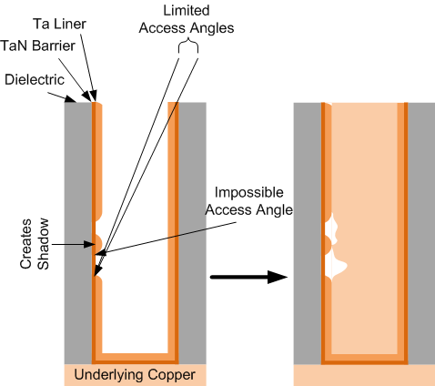
Figure 1. Imagining how voids could affect via fill.
Of course, it’s not this simple. One feature, wetting, helps by letting the metal spread out when it lands. So that blob on the left might actually flatten and cover more. And, even if it didn’t, that top part of the void, which can’t be directly reached, could be covered by metal landing below and then spreading up to cover the entire void. If the wetting is good enough, that is.
Obviously, my picturing of the resulting void on the right after the copper goes in is highly speculative. But hopefully it illustrates the point.
With the bigger vias we’ve historically had, the barrier and liner layers can be thicker, and thicker layers are less likely to have voids simply because there’s more material mooshing around. But smaller vias mean a thinner tantalum film – compounding the coverage problem.
Your metal is on the move
Before we jump to AMAT’s specific solution to this, let’s talk about another source of metal voids: metal lines. And there are two problems. One is increased trench edge roughness, making good barrier and liner coverage harder. It’s like the via in Figure 1, although I haven’t included roughness in that figure.
But there’s a second source: metal lines that don’t make a good, solid bond with the dielectric above them. Higher current densities in thinner metal wires increase the risk of electromigration, and copper that doesn’t stick well to the layer above it can move, creating voids in the places it abandoned. These two metal line challenges are illustrated in Figure 2.
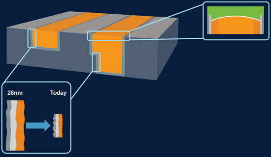
Figure 2. Edge roughness and top dielectric adhesion are challenges. (Image courtesy Applied Materials)
One of the ways of dealing with the adhesion problem is to seed the copper with another metal, like manganese or aluminum, during deposition. When capped with dielectric, those atoms tend to migrate upwards and bind to the interface. They apparently can also help to plug tantalum voids on the side. The challenge is that some of those alloy atoms remain in the copper – they don’t all migrate to the edge, and that reduces the conductivity.
OK, so, given all of these issues, Applied Materials is proposing a solution that can be summarized in one word: Cobalt (Co). There are two reasons why they think this is a good idea. First, it wets better; second, it adheres better to the dielectric.
In other words, after the TiN barrier deposition, you line the via with cobalt instead of tantalum. Thanks to better wetting characteristics, it can spread more readily and provide better coverage. This addresses the integrity of the sidewalls and bottom for both vias and metal trenches.
But they also propose using it as a cap over the metal lines after CMP. And this warrants further examination. When trenches and vias are filled with metal, copper is lavishly laid over everything to ensure a good fill. Left like that, everything would be shorted over the entire die due to the layer of copper on top of everything. CMP grinds that copper down until the excess is gone – that is, until you’re grinding into the dielectric, leaving the copper only inside the trenches.
So far, so good. But now, after this step, AMAT is proposing laying down a thin layer of cobalt as a cap. And if it were done like the copper is done, then you’d have this complete metal layer of cobalt over the entire die, just like you had with copper before CMP. The thing is, you can’t use CMP now – you’ve already ground the copper flush with the dielectric sides, so if you ground the cobalt down to that same level, you’d eliminate all the cobalt.
Another option would be to use a masking step to get rid of the excess cobalt – that is, making sure that it follows only the metal lines as a cap and that, critically, it never bridges two metal lines over the dielectric that separates them. But that’s another masking step –expensive – and metal overlay would be critical to making sure that the masked cobalt remained exactly on top of the copper, leaving no corners of copper uncovered and no excess pileups of cobalt on dielectric due to slight mis-registration between the cobalt mask and the trench mask.
Well, here’s where AMAT claims to have a trick up their sleeves – the details to which I am not privy. They have a way of selectively depositing the cobalt. In other words, there’s some way they can expose the entire wafer surface to the cobalt during deposition – possibly involving how they prepare the cobalt compound or how they pre-treat the die surface or both – that means that the cobalt will stick only to the copper. Importantly, it won’t stick to the dielectric. No mask/etch required.
This means that, with no extra masking step, you get, by definition, perfect alignment of the cobalt with the underlying copper and, presumably, a perfect cap. Combined with the sidewalls and bottom barrier layers, the copper is now completely surrounded by cobalt, touching neither silicon nor trench dielectric nor overlaying dielectric.
By the way, IBM did some experiments with both ruthenium (Ru) and cobalt. According to the report, Ru has better wetting, but doesn’t polish well – especially with copper. So cobalt got the nod.
AMAT has announced this new CVD capability in a way that allows cobalt deposition within a new chamber attached to the same module that’s used for Ta and TaN deposition when filling vias. Selective deposition after CMP is a separate step. These two depositions (per metal layer) are the only modifications to the process flow, mitigating the extra cost of adding cobalt to the process.
Metal changes are a big deal; they don’t happen often. We’ll have to see if this becomes the accepted solution at these nodes or whether others propose different solutions to these problems. If you know of alternatives, be sure to comment below.
More info:
IBM paper describing detailed experiments (behind paywall)


Do you think cobalt is the right solution to the problem of filling vias and getting metal to stick to the dielectric cap?