

[Editor’s note: this is the second in a series of articles derived from a session at this year’s ISSCC that focused on sensors and energy harvesting. The prior article dealt with wind sensors. For more details you are referred to the ISSCC proceedings.]
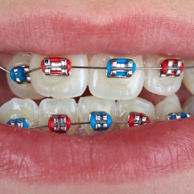
Nobody likes braces. They look funny, they limit what you can eat, and, worst of all, they can hurt. And they’re expensive.
While it looks like braces are simply a line of brackets with a single wire pulling them all in one direction, it’s much more complex than that. Each tooth has an individual trajectory to get from where it is to where you want it. That can mean moving it in any direction and often rotating it. Tough to do with such a tiny apparatus.
It’s the orthodontist’s job to make sure that the forces are all being applied in the right ways to make this happen. But they can measure the forces only in one dimension, when, in fact, many dimensions are needed.
It’s almost like you need an individual embedded system on each tooth to measure and calculate the forces being applied in all directions on that tooth.
Well, don’t laugh. That’s exactly what was presented at ISSCC by a team from the University of Freiburg and the Institut für Mikro- und Informationstechnik (HSG-IMIT). It’s not a big system, but it does combine the necessary sensing elements with a way to transmit the information wirelessly to a reader that the orthodontist would place near each tooth during a checkup.
Before we can walk through the system they implemented, we need to deal with some fundamentals on how the forces being applied can be measured by a chip. And we’ll start pretty basic, just for safety, with apologies to anyone for whom this is obvious.
When forces act on a body, they deform the body to some extent, limited by the internal resisting forces of the material being deformed. Silicon, for example, has a nice lattice crystal that represents a low-energy state. So the crystal will resist having those atoms pulled out of their cozy repose.
To be precise here, “strain” is the deformation of the material, which can be compressive (pushing the ends together) or tensile (pulling the ends apart). In addition, the strain can be caused by shear forces, where the force, say, presses on the end of a bar, but is stronger on the top than on the bottom, tending to turn the bar into a parallelogram (when viewed from the side). Or they can cause rotation, described by various odd-sounding phrases as “difference of moments.” Sounds more like the thing that happens at a bar when two people sharing a “moment” have a completely different understanding.
“Stress” is the amount of internal resistive force.
What follows is a distillation of lots of openly-available bits and pieces regarding silicon strain sensors. This stuff can get dense pretty quickly, so there’s a limit to how deeply I wanted to dive (much less describe here). Most of these concepts are spread far and wide, and tying them together is something of a leap of faith. This is how I make sense of it.
When you apply a force against a crystalline material, it can cause various effects. Some materials, having an electrically asymmetric lattice, undergo the “piezoelectric” effect, where moving charges can be detected. Silicon is not one of those materials, however: it has a symmetric structure.
Silicon does exhibit what’s caused the “piezoresistive” effect: essentially, when the forces are applied, the mobility changes because the atoms in the lattice are getting closer together or farther apart, changing the resistance. This is the basic idea behind the so-called “strain engineering” used for improving transistor performance.
This change in resistance can be detected and used as a measure of strain. For silicon, there’s lots of math that’s been done to calculate strain, and it depends on the crystal orientation. It boils down to a number of coefficients that are needed. Once known, they can be plugged and chugged and the strain pops out. For [100] wafers there are four coefficients, and, for [111] wafers, there are six.
In order to measure the forces, resistors are laid out in different directions. The arrangement of resistors is called a “rosette.” It’s like an n-equations/n-unknowns problem. For the four coefficients in [100] silicon, a four-resistor rosette is used. For [100], you need six, but eight are typically used because you can use a Wheatstone bridge arrangement to measure them more easily.
But… it gets more complicated. Apparently, if you want to take any orientation into account, then, for a given constant doping level, you can get only three unique responses out of the six- (or eight-) resistor rosette. So to deal with this, one eight-resistor rosette is replaced by two four-resistor rosettes, one using n-type silicon, the other using p-type. The two are oriented 45° from each other.
Each rosette is a sensor. This pair of rosettes is the workhorse of silicon strain sensing.
Getting back to the actual orthodontic problem at hand, these sensors needed to be positioned on a chip that would be mounted to the actual tooth bracket. They used mechanical finite-element analysis to figure out where the stresses (or strains?) were on the chip based on the underlying bracket mechanics; this gave them the sensor positions. They used a total of 24 stress sensors.
They located the rest of the circuitry in low-stress areas of the chip; after all, if strain is changing the resistors in the sensors, then it could be having an effect on the circuits too. Best to minimize that.
There is another source of inaccuracy that they had to deal with: there could be systematic variations as well as noise that could cause the rosettes not to be completely symmetric. In order to correct for this, they added the ability to “rotate” the rosettes. Not physically, of course, but they used a multiplexor to change which “poles” of the rosette were interpreted as which, changing by 90° at a time. Over time, any error or noise gets averaged out. The rotation happens at 10 Hz, meaning a shift every 100 ms.
They use a differential difference amp (DDA) (which has a name that makes as much sense as a “repetitive repeater circuit”). One of those million-dollar names that’s less scary than it sounds: it’s simply an op amp that has differential inputs instead of the “normal” single-ended inputs.
But the trick here was to set the gain on the DDA in a manner that would allow a broad range of accurate measurements. To do this, they used an “auto-scaling” circuit that would measure the output, and, if it wasn’t pegged at the top, they’d go to a higher gain until it did peg, and then back off. This meant that each measurement would be read with the highest possible gain useable for that particular measurement. The entire process – readout, gain adjustment, and settling – takes 600 µs.
The result, after converting to digital, is a 22-bit value. That value is then transmitted to the reader using amplitude shift keying (ASK) – basically, digital AM: the carrier is full on for, say, a 1 and completely suppressed for a 0.
Acquisition and transmission of all 24 sensors takes 530 ms.
There’s one more important piece of this system: power. It’s not plugged in. It occurs to me that a battery charging system harvesting the energy of chewing would be most excellent. Except for the toxic chemicals in a battery… (maybe someone will figure that out). That’s not how this was handled.
The sensor chip is powered by a near-field signal from the reader that the orthodontist uses. To capture that, a coil was deposited on a pyrex wafer, which was sliced up to the same size as the sensor chip and mounted to it with flip-chip connections.
The power-on circuit has hysteresis built in – it takes more energy to get the thing going, but once on, it will operate to a much lower voltage. They put two voltage limiters in place: a coarse one that protects things during the early part of power-up and a fine one that takes over once the bandgap regulators and such are up and running.
The power conversion isn’t constant. The system cycles through three steps: charge the buffer cap, read a sensor, transmit the sensor results, and then repeat with the next sensor. Enough power is provided by the reader, up to 2 mm away, to enable the circuit to wake up, make the measurements, and transmit them.
And there you have it. A 2-mm x 2.5-mm chip/coil sandwich that mounts to a tooth bracket and can tell the orthodontist exactly what forces are at play in all directions. I wonder if, with better data, and therefore better control, the braces will hurt less. I’m not betting on it. It does seem reasonable that they might shorten the duration of the torture.
But at least, when the price of braces goes up because now they’re smart, you will know just what is going on inside the little buggers. I’m sure that will reduce the financial pain.
(Note: you can find the next article in the series here.)


7 thoughts on “Smart Braces”