feature article
Subscribe Now

Denali Announces State-of-the-Art GHz DDR PHY Technology

SUNNYVALE, Calif., Dec. 10 /PRNewswire/ — Denali Software, Inc., a world-leading provider of electronic design automation (EDA) software and intellectual property (IP), today revealed a new phase PHY technology for DDR SDRAM physical interfaces, delivering memory system performance up to 1066 MHz clock speeds (or DDR-2133 data rates) on 65-nanometer foundry process nodes or lower. Denali’s phase PHY technology applies a high-speed oversampling architecture paired with per-bit data capture and calibration mechanism to achieve GHz clock rates. This third-generation DDR PHY technology is delivered as a fully-synchronous design which benefits design teams with the configurability needed to satisfy their physical implementation requirements.

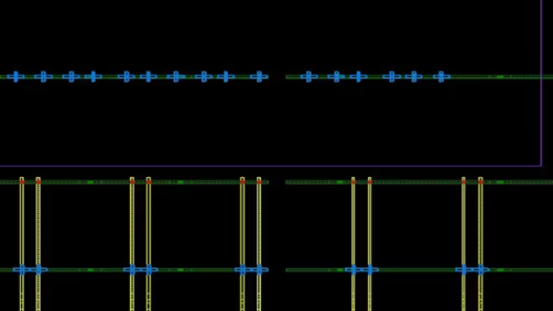
As DDR SDRAM devices reach 2133 Mbps data rates, bit-to-bit skews within the data lanes become significant fractions of the data window. Denali’s oversampling architecture employs an 8- or 16-phase lock loop (PLL) and performs pattern matching to determine the correct data sample points for DDR data for each transaction. By managing the data capture on a per-bit basis (rather than on a per-byte basis), Denali’s PHY reliably closes timing at 1066 MHz clock rates. Furthermore, differences in the routing of data and data strobe signals are calibrated in the silicon eliminating the need for time-consuming hand layout. The fully-synchronous design provides flexibility for floorplanning, pin placement, and power routing and uses standard EDA toolsets to easily realize a reliable implementation.

“The continued demand for increased bandwidth in various internet and electronic applications is driving the need for DDR3 technology and for the ability to support data rates up to 2133 Mbp/s,” states Mike McKeon, director of PHY IP at Denali. “Our DDR phase PHY is cutting-edge technology, delivering effective management of GHz clock speeds and a perfect match for our customers’ specific design implementation needs.”

About Databahn DDR PHY Solutions

Denali’s Databahn DDR PHY is a complete solution ready to be integrated into SoCs and ASICs which interface with DDR memories. Each PHY is delivered to match the unique requirements of the customer’s DDR application. The PHY is configurable for data width, ECC, low power, and many other options, and supports DDR3/2 and LP-DDR1/2 devices. For more info, visit: www.denali.com/ddrphy, Databahn PHY Frequently Asked Questions, and Animated Guide to Denali DDR PHY.

About Denali Software

Denali Software, Inc., is a world-leading provider of electronic design automation (EDA) software and intellectual property (IP) for system-on-chip (SoC) design and verification. Denali delivers the industry’s most trusted solutions for deploying PCI Express, USB, NAND Flash and DDR SDRAM subsystems. Developers use Denali’s EDA, IP and services to reduce risk and speed time-to-market for electronic system and chip design. Denali is headquartered in Sunnyvale, California and has offices around the world to serve the global electronics industry. More information about Denali, its products and services is available at www.denali.com.

Leave a Reply

Maia EDA Launches New Automated Verification Tool

CAMBRIDGE, England–(BUSINESS WIRE)–Maia EDA has today announced the availability of the Maia functional verification tool. Maia uses a description of the expected behavior of a device to automatically create a complete self-checking reactive testbench, so freeing engineers from the time-consuming, complex, and error-prone task of manual testbench creation. The tool has been designed to enable both engineers and non-engineers to quickly verify modules and sub-systems, and is initially being offered without cost by the company, allowing trial without registration or risk.

Maia is primarily targeted at hardware engineers who write and need to verify their own RTL code, but a key benefit of the tool is that it can be used by staff who have no knowledge of Verilog or VHDL, and who have only minimal programming skills. Modules and subsystems can be verified by anyone who has access to a specification, and who can construct sequences of vectors corresponding to the device inputs, and expected outputs.

“Module verification is normally carried out by the same hardware engineer who designed the module. The engineer is expected to hand over a working module,” commented Evan Lavelle, CTO of Maia EDA. “However, engineers are not usually programmers, and are unlikely to have the mindsets, or the time, which are required to create complex and exhaustive verification programs. The result is frequently that FPGAs are tested and debugged in-system, and ASIC developers have to buy complex system-level verification tools to find problems that should have been caught at a lower level. It’s also a fact that most engineering companies don’t have the resources to hire dedicated verification staff anyway. This is where Maia fits in.”

Maia automates the creation of testbenches by using declarative and fifth-generation language (5GL) techniques. An expected ‘solution’ is specified by listing sequences of inputs and expected outputs as vectors. Maia treats the vectors as constraints, and creates the corresponding self-checking testbench, automating the processes of driving and testing timed device inputs and outputs, clock and reset generation, stability checking, pipeline handling, internal signal probing and forcing, time handling, and error reporting.

Maia can be downloaded without charge from: http://maia-eda.net.

About Maia EDA

Maia EDA is a Cambridge-based EDA startup. The Maia language arose out of the need to create practical verification tools for real-world design, rather than esoteric system-level tools that have little or no relevance to working Electronic Engineers.

The founders have extensive experience of the design and verification of ASIC and FPGA devices, as well as the development of complex compilers and toolchains for automated verification environments. The initial need was identified while carrying out hardware development, during which it was obvious that there was a disconnect between the needs of engineers and the available tools. This realisation led to the development of an automated testbench generator, which was constantly refined and tested on a large number of real designs, by real engineers, over several years. This proven technology has now been commercialised by Maia EDA.

Leave a Reply

featured blogs
May 2, 2025
I can safely say that I've never seen a wheeled-legged robot that can handle rugged terrains, muddy wetlands, and debris-strewn ruins like this...

featured paper

How Google and Intel use Calibre DesignEnhancer to reduce IR drop and improve reliability

Sponsored by Siemens Digital Industries Software

Through real-world examples from Intel and Google, we highlight how Calibre’s DesignEnhancer maximizes layout modifications while ensuring DRC compliance.

Click here for more information

featured chalk talk

How to Choose the Right Battery Charger
Sponsored by Mouser Electronics and MEAN WELL
In this episode of Chalk Talk, Thrax Cui from MEAN WELL and Amelia Dalton explore how you can choose the right battery charger for your next design. They investigate the battery charging principles of lithium ion and lead acid batteries, the steps involved in choosing a battery charger, and how MEAN WELL battery charging solutions support the charging needs of a wide variety of applications.
Apr 29, 2025
3,630 views