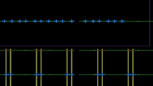
LEUVEN, Belgium and SAN JOSE, Calif., June 6, 2011—Imec, a world-leading nanoelectronics research institute based in Belgium, and Cadence Design Systems, Inc. (NASDAQ: CDNS), a leader in global electronic design innovation, today announced new technology that delivers an automated test solution for design teams deploying 3D stacked ICs (3D-ICs). The technology addresses the test challenges involved as electronics companies increasingly turn to 3D-ICs as a way to increase circuit density and achieve better performance at lower power dissipation for mobile and other applications where space is at a premium.
This imec-Cadence collaboration provides the design-for-test (DFT) and automatic test pattern generation (ATPG) technology that will make it easier to test 3D-ICs with “through-silicon via” (TSV) functionality and help ensure that the stacked system will work as intended.
Insights gained during its comprehensive research program on TSV-based 3D-IC design and technology enabled imec to extend the DFT architecture for conventional (2D) ICs with several novel (patent-pending since Q1 2010) features. The 3D DFT architecture is based on the concept of die-level test wrappers, which enable testing of chips with TSVs and micro-bumps both before (“pre-bond test”), during (“mid-bond test”), and after (“post-bond test”) stacking, as well as after packaging.
“This new DFT solution is the latest example of our commitment at Cadence® to the emerging area of 3D-IC,” said Brion Keller, senior architect at Cadence. “Over the past two years, we’ve introduced 3D-IC TSV and silicon interposer capabilities, and, just three months ago, the industry’s first wide I/O memory controller IP solution, with a robust 3D-IC integration environment. Collaboration is an essential element of effective Silicon Realization and the EDA360 vision we adhere to, and this initiative with imec demonstrates why.”
“Using 3D-IC and TSV technology, electronics companies look forward to creating a new generation of super chips,” said Erik Jan Marinissen, principal scientist at imec. “The imec-Cadence offering inserts DFT structures with minimal area overhead, and the ATPG method helps drive towards zero manufacturing defects on the TSVs. This unique offering reduces risk and promotes cost-effective fabrication of these chips.”
Cadence and imec created the design flow automation for adding 3D-enhanced IEEE 1500-based die wrappers to existing chip designs. This was done by enhancing the existing IEEE 1500 wrapper insertion support in the Cadence Encounter® RTL Compiler synthesis product. Initial results on customer designs showed that the 3D DFT structures can be implemented with negligible area costs—about 0.2%, which is far less than what some in the electronics industry have been speculating.
About imec
Imec performs world-leading research in nanoelectronics. Imec leverages its scientific knowledge with the innovative power of its global partnerships in ICT, healthcare and energy. Imec delivers industry-relevant technology solutions. In a unique high-tech environment, its international top talent is committed to providing the building blocks for a better life in a sustainable society. Imec is headquartered in Leuven, Belgium, and has offices in Belgium, the Netherlands, Taiwan, US, China and Japan. Its staff of about 1,900 people includes more than 500 industrial residents and guest researchers. In 2010, imec’s revenue (P&L) was 285 million euro. Further information on imec can be found at www.imec.be.
About Cadence
Cadence enables global electronic design innovation and plays an essential role in the creation of today’s integrated circuits and electronics. Customers use Cadence software, hardware, IP, and services to design and verify advanced semiconductors, consumer electronics, networking and telecommunications equipment, and computer systems. The company is headquartered in San Jose, Calif., with sales offices, design centers, and research facilities around the world to serve the global electronics industry. More information about the company, its products, and services is available at www.cadence.com.


