feature article
Subscribe Now

MoSys and CEVA Partner to Deliver Integrated SATA 3.0 PHY and Controller IP Solution

SUNNYVALE, CA and SAN JOSE, CA, June 9, 2010 — MoSys, Inc. [NASDAQ: MOSY], a leading provider of differentiated, high-density memory and high-speed interface (I/O) intellectual property (IP), and CEVA, Inc. [NASDAQ: CEVA]; [LSE: CVA], the leading licensor of silicon intellectual property (SIP)  DSP cores, multimedia and storage platform solutions, have partnered to deliver a joint PHY plus Controller solution for  SATA 3.0, for both Host and Device side applications. 

The combined solution unleashes the full potential of embedding 6Gbps SATA interfaces in next generation products by leveraging MoSys’ 6Gbps SerDes PHY and CEVA’s SATA 3.0 Controller IP.  By co-operating  to provide proven interoperability  and direct engineering assistance, MoSys and CEVA will help SATA designers speed time-to-market, as well as reduce costs and risks when integrating SATA 3.0.  In addition to strong technical collaboration, MoSys and CEVA will also partner to jointly market their new, integrated SATA 3.0 PHY and Controller IP solution.

“CEVA has an influential history in Serial ATA. Their recently announced SATA 3.0 solution is the perfect complement to our SerDes PHY. By combining our technical expertise, we have created a state of the art solution that should come up smoothly and faultlessly for our shared customers,” said David DeMaria, Vice President of Business Operations at MoSys. “We are delighted to be working with CEVA.”

“Our latest generation SATA 3.0 Controller IP builds on the highly popular CPU off-loading features of the CEVA-SATA 2.6 Controller to provide enhanced NCQ for isochronous data transfers and queue management,” said Aviv Malinovitch, Vice President, Operations at CEVA. “We are very pleased to expand the eco-system and choices for customers by partnering with MoSys, and we look forward to a long-term partnership.”

Information and further details about the integrated SATA 3.0 solution are available from both companies. Contact MoSys at www.mosys.com/contact.php and CEVA at info@ceva-dsp.com.

About MoSys, Inc.

MoSys, Inc. (NASDAQ: MOSY) develops serial chip-to-chip communications solutions that deliver unparalleled bandwidth performance for next generation networking systems and advanced system-on-chip (SoC) designs. MoSys’ IP portfolio includes DDR3 PHYs and SerDes IP that support data rates from 1 – 11 Gigabits per second (Gbps) across a variety of standards. In addition, MoSys offers its flagship, patented 1T-SRAM® and 1T-Flash® memory cores, which offer a combination of high-density, low power consumption, high speed and low cost advantages for high-performance networking, computing, storage and consumer/graphics applications. MoSys IP is production-proven in more than 225 million devices. MoSys is headquartered in Sunnyvale, California. More information is available on MoSys’ website at www.mosys.com.

About CEVA, Inc.

CEVA is the leading licensor of silicon intellectual property (SIP) DSP Cores and platform solutions for the mobile handset, portable and consumer electronics markets. CEVA’s IP portfolio includes comprehensive technologies for cellular baseband (2G / 3G / 4G), multimedia, HD audio, voice over packet (VoP), Bluetooth, Serial Attached SCSI (SAS) and Serial ATA (SATA). In 2009, CEVA’s IP was shipped in over 330 million devices, including handsets from 7 out of the top 8 handset OEMs, including Nokia, Samsung, LG, Motorola, Sony Ericsson and ZTE. Today, more than one in every four handsets shipped worldwide is powered by a CEVA DSP core. For more information, visit www.ceva-dsp.com.

Leave a Reply

TOOL Corp. Announces New Release to Layout Visualization Platform, LAVIS

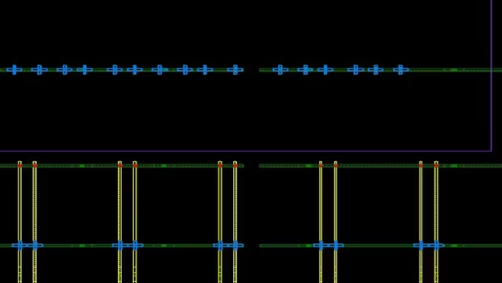
Tokyo, Japan – June 11, 2010 – TOOL Corporation (headquarters in Tokyo Japan, president Hideaki Hontao) announced the release of LAVIS Version 10.0, their layout visualization platform software. In this version, the new “Route Trace function” has been incorporated that makes it possible to display timing information and easily and visually check the clock tree and other elements. The node tracing function, which allows wire width, inter-node spacing, and other rule checks to be made on a traced node, has been improved as well. These and other enhancements make LAVIS even more useful in reducing design TAT.

In this version, a great variety of functions have been added and existing functions have been enhanced.  The main additions and enhancements are described below.

(1) Addition of the Route Trace function 

The new “Route Trace function” has been incorporated that allows efficient route tracing from a specified component in LEF/DEF data. This function is very useful in checking a route that has caused a timing violation as well as in narrowing down routes to find the faulty one.

(2) Expansion of the node tracing function

As part of the node tracing function, a new function has been added that automatically detects a location where the resistance becomes high at the contact connection point. This function makes it easy to check whether the resistance assumed as an electrical characteristic is realized at a contact point.

(3) Expansion of the width/spacing measurement functions

The measurement function automatically judges whether figures are present or not at measured points, enabling measurement results to be output in a way that distinguishes between L and S. Also, at the request of the customer, an optional function can be offered separately that automatically measures the width and spacing of multiple locations based on given coordinates.

In addition to the above, a number of function expansions have been made, including the
addition of a new measurement function that measures the distance between centers of
multiple figures, the inclusion of a marker grouping function that lets you change the colors and widths of multiple markers or move them simultaneously, the support for OASIS data for the logical operation function, and the enhancement of the optional simple edit and 3D view
functions.

Hideaki Hontao, president of TOOL, said, “In this version upgrade, we have added functions that enable LAVIS to be used as an auxiliary tool for timing and fault analysis as well. We intend to continue to determine customer needs accurately and promptly in the future, and add more functions and expand existing ones so that customers can use LAVIS in various fields.”

About LAVIS

LAVIS is a versatile and ultra-high speed layout visualization platform that supports large data and multiple file formats. Its unique display method, coupled with memory management technology, efficiently enables large volume data handling and fast display. Most importantly, LAVIS can be used as a common standard layout platform for all the IC processes such as design, verification, mask data preparation, inspection and failure analysis, thanks to its capability to support various data formats, including GDS, OASIS, LEF/DEF and e-beam thereby making it easy to interface with other tools for the entire IC making flow.

About TOOL

TOOL is a Japanese software development company focused primarily on EDA tool development. Its particular strength is in the area of layout design, and has scored a number of achievements in this area with its development tool, LAVIS and MaskStudio. Solutions to chipmakers’ problems can be provided by combining TOOL’s package-software with its custom-tailored software developed to serve a customer’s particular need. TOOL provides ample experience in this particular area. For more information on TOOL and products, please refer to
http://www.tool-corp.com/

Leave a Reply

featured blogs
Nov 12, 2024
The release of Matter 1.4 brings feature updates like long idle time, Matter-certified HRAP devices, improved ecosystem support, and new Matter device types....
Nov 13, 2024
Implementing the classic 'hand coming out of bowl' when you can see there's no one under the table is very tempting'¦...

featured video

Introducing FPGAi – Innovations Unlocked by AI-enabled FPGAs

Sponsored by Intel

Altera Innovators Day presentation by Ilya Ganusov showing the advantages of FPGAs for implementing AI-based Systems. See additional videos on AI and other Altera Innovators Day in Altera’s YouTube channel playlists.

Learn more about FPGAs for Artificial Intelligence here

featured paper

Quantized Neural Networks for FPGA Inference

Sponsored by Intel

Implementing a low precision network in FPGA hardware for efficient inferencing provides numerous advantages when it comes to meeting demanding specifications. The increased flexibility allows optimization of throughput, overall power consumption, resource usage, device size, TOPs/watt, and deterministic latency. These are important benefits where scaling and efficiency are inherent requirements of the application.

Click to read more

featured chalk talk

SiC-Based High-Density Industrial Charger Solutions
Sponsored by Mouser Electronics and onsemi
In this episode of Chalk Talk, Amelia Dalton and Prasad Paruchuri from onsemi explore the benefits of silicon carbide based high density industrial charging solutions. They investigate the topologies of Totem Pole PFC and Half Bridge LLC circuits, the challenges that bidirectional CLLC resonant DC-DC converters are solving today, and how you can take advantage of onsemi’s silicon carbide charging solutions for your next design.
May 21, 2024
37,609 views