fresh bytes
Subscribe Now

The ‘world’s biggest’ 3D printer will build emergency houses

BigDelta12m.jpg

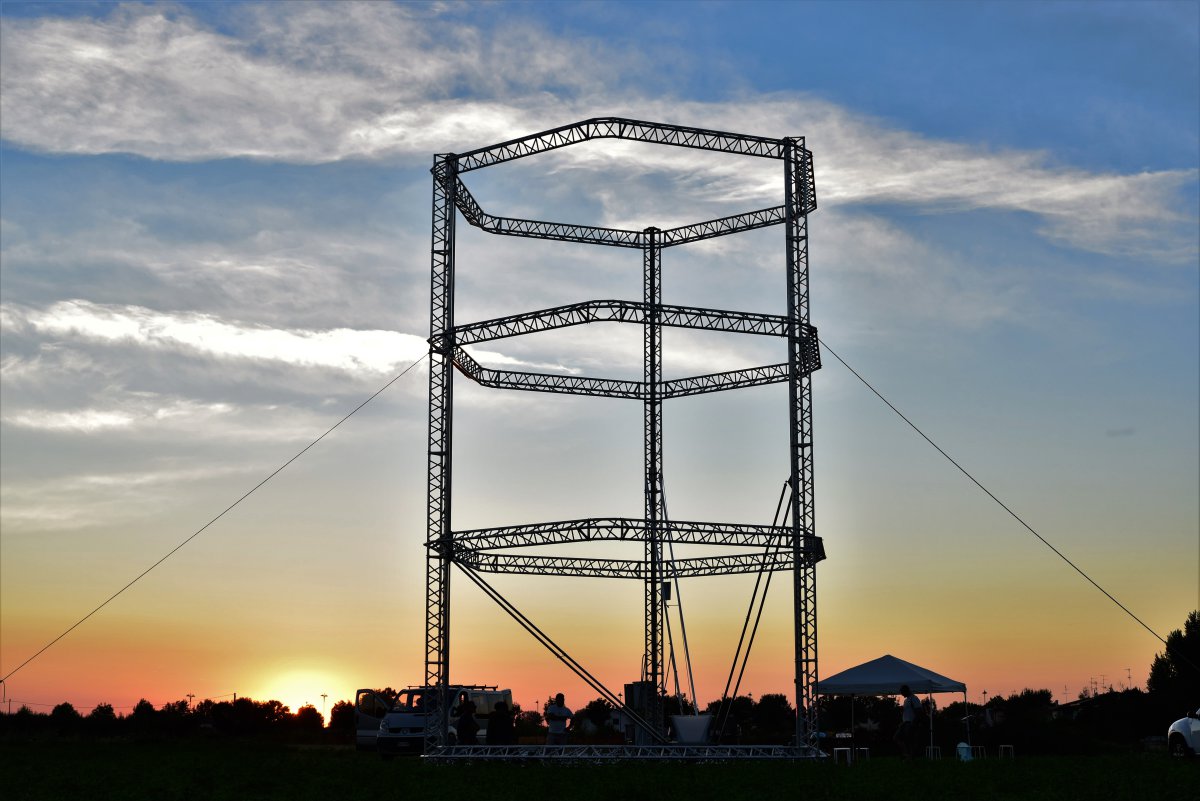
The design team at WASP (World’s Advanced Saving Project) will unveil what is being billed as the world’s largest 3D printer on Friday in Rieti, Italy. Dubbed the “Big Delta,” this enormous device stands roughly 40 feet tall with a 20 foot diameter. But despite its size, the Big Delta is extremely efficient and uses only 100 watts of power. Its oversized design allows the Big Delta to quickly and easily print low-cost disaster-relief housing. What’s more, it can do so using locally-sourced materials (read: dirt and mud) which also acts to minimize construction costs. The WASP team also foresees employing this printer for non-disaster-related home building. According to a company release, the Big Delta help accommodate the estimated 4 billion people worldwide that will lack adequate housing by 2030.
via Engadget

Continue reading 

Leave a Reply

featured blogs
May 2, 2024
I'm envisioning what one of these pieces would look like on the wall of my office. It would look awesome!...
Apr 30, 2024
Analog IC design engineers need breakthrough technologies & chip design tools to solve modern challenges; learn more from our analog design panel at SNUG 2024.The post Why Analog Design Challenges Need Breakthrough Technologies appeared first on Chip Design....

featured video

MaxLinear Integrates Analog & Digital Design in One Chip with Cadence 3D Solvers

Sponsored by Cadence Design Systems

MaxLinear has the unique capability of integrating analog and digital design on the same chip. Because of this, the team developed some interesting technology in the communication space. In the optical infrastructure domain, they created the first fully integrated 5nm CMOS PAM4 DSP. All their products solve critical communication and high-frequency analysis challenges.

Learn more about how MaxLinear is using Cadence’s Clarity 3D Solver and EMX Planar 3D Solver in their design process.

featured paper

Achieve Greater Design Flexibility and Reduce Costs with Chiplets

Sponsored by Keysight

Chiplets are a new way to build a system-on-chips (SoCs) to improve yields and reduce costs. It partitions the chip into discrete elements and connects them with a standardized interface, enabling designers to meet performance, efficiency, power, size, and cost challenges in the 5 / 6G, artificial intelligence (AI), and virtual reality (VR) era. This white paper will discuss the shift to chiplet adoption and Keysight EDA's implementation of the communication standard (UCIe) into the Keysight Advanced Design System (ADS).

Dive into the technical details – download now.

featured chalk talk

Extend Coin Cell Battery Life with Nexperia’s Battery Life Booster
Sponsored by Mouser Electronics and Nexperia
In this episode of Chalk Talk, Amelia Dalton and Tom Wolf from Nexperia examine how Nexperia’s Battery Life Booster ICs can not only extend coin cell battery life, but also increase the available power of these batteries and reduce battery overall waste. They also investigate the role that adaptive power optimization plays in these ICs and how you can get started using a Nexperia Battery Life Booster IC in your next design.  
Mar 22, 2024
6,245 views