You may remember that, early this year, we took a look at a 1-transistor (1T) SRAM bit cell. (Yes, new memory stuff seems all the rage lately – and we’re probably not done yet.) Well, there’s another story evolving out of that 1T cell, only it’s not related to memory. It’s related to one of the most fundamental devices in our toolkits: the transistor itself. Zeno claims that they can boost the drive current of an ON transistor by two times – something that would ordinarily take several process nodes to achieve. And all without increasing leakage – something several process nodes would not likely be able to provide.
They call it βMOS, with “beta” standing for “boosted.” And they found it more or less by accident while characterizing their 1T bit cell. So let’s start by reviewing that cell.
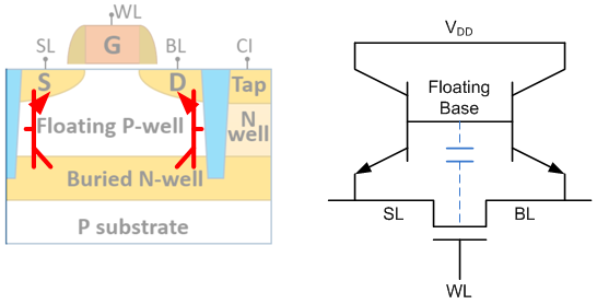
The idea is that, with a buried n-well below the MOS channel at an elevated voltage and an isolated, floating p-well above it, you transform the lowly MOS transistor into a more complex beast that includes two npn bipolar transistors, with the buried n-well acting as the collector.

(Left image based on an image courtesy Zeno)
By raising the gate of the MOS transistor (controlled by the word line) quickly enough, you couple to the floating p-well, which forms the base of the bipolar transistors. This pumps up the base and gets current flowing through the collector, and it becomes self-sustaining in a way that can be interpreted as a state – hence its use as a memory cell.
If this were your cell, you’d naturally be playing with all the voltages and other conditions to circumscribe the conditions under which this works. And one of those voltages is the level to which the buried n-well is raised – in other words, what range of voltage on the collector ensures reliable reading, writing, and storage?
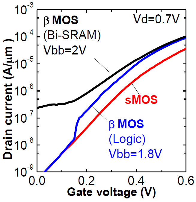
During that characterization, Zeno found a peculiar thing. With the n-well biased at around 2 V, it behaved as expected for the bit cell. We look at this test in the next figure, where we see the I/V curves. The top black line represents the 1T bit cell, and it has high drive at both the low and the high end of the voltage range.
A standard MOS device (which they refer to as sMOS), has lower leakage current because the bipolar transistors aren’t making their contribution; that’s shown in red below. But a funny thing happens when you dial that buried n-well voltage lower: when the gate voltage is high, it acts like the 1T bit cell, with extra drive current. But with a low gate voltage, it acts like the sMOS transistor. In fact, if you scan from left to right, what they’re calling the βMOS curve (blue) starts out overlayed on the sMOS curve, but, at some point, it departs from that curve and joins the 1T curve. What’s going on here?

(Image courtesy Zeno)
Well, the first thing that’s not going on is memory. Below whatever that Vbb limit is (here, somewhere between 1.8 and 2 V), there’s just not enough current to get the memory state established. You get current, but it’s not self-sustaining, so it goes away when the gate voltage is brought back down.
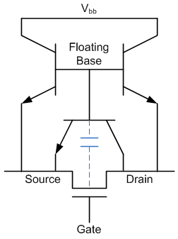
In analyzing this, Zeno has postulated a reasonably complex mechanism at work, and it involves yet another parasitic npn – this time between source and drain, with the buried p-well acting as its floating base (just as it does for the two vertical npns).

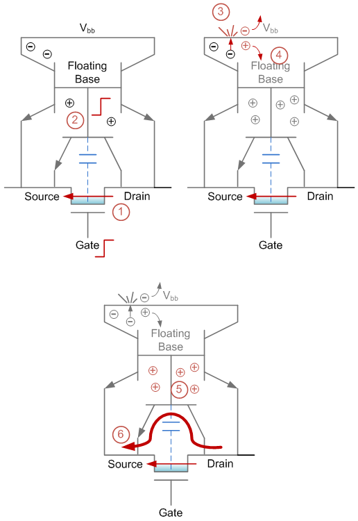
Looking at that, you might be tempted to say that it’s simply the lateral npn being turned on by the coupled floating base while the drain voltage is high. But it’s apparently not that simple, since you need some mechanism that accounts for sufficient holes in the base region. Here’s the sequence of events that they propose:
- First, the MOS transistor turns on, creating inversion in the channel.
- Next (or, really, simultaneously), the vertical bipolar transistors turn on, as with the 1T bit cell. This gets current flowing through the buried n-well. This means that electrons are moving up to the collector (in the above transistor drawing, that is – in the silicon drawing, they’re moving down to the buried n-well).
- When the electrons hit the buried n-well junction, they do so with enough energy to cause impact ionization. This creates free electron-hole pairs, and the electrons are swept into and out of the collector, while the holes…
- … move to the base region where they…
- … stimulate the lateral bipolar transistor to turn on more.
- This provides a second path for current from the drain to the source, bypassing the normal MOS channel and arriving via the lateral npn. Hence higher-than-normal drive.

What’s interesting here is the source of the additional current. With the 1T bit cell, that extra current comes from the collector of one of the vertical npns. But in this case, it’s coming from the drain of the MOS device via the lateral npn.
Of course, they’re still characterizing this phenomenon, but if it survives the scrutiny, then, well, it seems like this would be huge. They say it can be applied to any process node that uses shallow trenches. They’ve run 28-nm planar transistors that work, and they’ve simulated FinFETs to show that it helps them as well.
In other words, it’s a giant jump ahead without having to resort to expensive techniques like nano-wires or tunnel FETs or other fancy stuff.
Almost sounds too good to be true – and, in fact, it occurred to me that there’s one aspect of this innovation that’s easy to lose track of: this is an AC phenomenon. It relies on the gate rising quickly enough to couple effectively to the floating base.
This is a more important consideration for this embodiment of the technology than it is for the 1T cell. If a memory cell needs a specific, controlled slew rate to work, then it’s expected that this requirement will be worked into (in this case) the word line driver requirements, and it will be built into the IP. But if your basic transistor is going to leverage this phenomenon, then every designer could be using it in any given situation.
While slew rate is a factor in standard design, it’s more of an AC consideration as part of a critical speed path. When considering the DC characteristics like drive, it’s not so common that you have to think through whether or not the driving slew rate will be sufficient to kick in the boost drive.
Of course, if one of these is driving another a short distance away, the very fact of boosted drive makes it more likely that you’ll get the rise rate you need. But what if you’re driving long lines? Will the transistor gates at the end of those long lines detect a watered-down rise rate that keeps them from achieving boost? Will this become a new consideration for designers and design tools?
That depends on what the minimum rise rate is that’s necessary to enable the boost feature. If, say, a 100-ns rise or a 1000-ns rise can still work, then that might be far enough outside the range of realistic expectations that you don’t really need to worry about it. But if the limit is, say, 10 ns, is that too close for comfort?
I asked Zeno about this, and CEO Yuniarto Widjaja noted that they’ve made many of their measurements using rise rates of 1 V per 100 ns. They’ve also been doing TCAD simulations, and they still see the boost effect at rise rates of 1 V per 2 ms (and I double-checked with them to confirm that this is indeed ms, not µs… in other words, these rise times are roughly a million times slower than the normal ns timescale). That last rate in particular is way slower than normal switching speeds, so that should put the matter to rest.
The other thing to note is that this feature solves what’s largely a digital problem. I can’t imagine this being helpful for analog design. You would have one more knob to dial and characterize (the buried n-well bias voltage), and the control of the I/V curve would have to be much more precise and controlled.
We saw above where, in essence, the I/V curve switches from the sMOS curve to the 1T curve as voltage sweeps up. For a digital design, it doesn’t really matter specifically where that switch happens. But if you’re going to use this for analog, that’s a new characteristic that has to be precisely controlled. Add to this the fact that this requires a jolt on the transistor gate to turn on the boost, and, well, I’m sure some creative analog wizard working very hard could find a way to leverage it, but it sounds impractical for everyday analog design.
Meanwhile, back in the digital world, if this makes it into commercial use, it could give the current process nodes a nice boost, keeping them relevant for longer and staving off the much-more-expensive advanced nodes.
More info:


What do you think of Zeno’s high-drive transistor boost?