


Astronomy bestows lavish breathless anticipation upon one of the great events of the universe: two galaxies running into (or through) each other. The thing is, it happens breathtakingly slowly – each stately galaxy spinning away, the distance between them slowly evaporating. Watching it is something of a sampling exercise: see where they are; nap for a couple of centuries. Wake, see that, yup, they’re a little closer; nap. Wake again, grab a new beer, and doggonnit if they aren’t just a wee bit closer yet. Basketball it’s not.
Well, we may have something of a similar event in play in EDA-land. Although referring simply to two galaxies isn’t quite fair: one, Synopsys, is perhaps more of a galaxy cluster to Coventor’s galaxy. To set the scene, let’s examine the status quo – the gap between the companies – and then we’ll look at each one to see how that gap is closing. And we’ll hopefully do it in a way that doesn’t involve napping.
If you’re not familiar with Synopsys, then you’re probably new to EDA. (Not judging…) An EDA behemoth, they’ve got strong positions in a number of areas – like multiple galaxies in a cluster. But the specific galaxy being challenged is one we hear little about, and it’s one that Synopsys totally dominates: TCAD. TCAD involves tools for simulating individual devices like transistors at an extremely detailed level.
It’s used when developing a technology, not when designing circuits on a technology. Once upon a time, it was the earliest category of tools in the lifetime of a semiconductor process, used for creating, with the help of wafer data, SPICE decks and PDKs that provide higher-level abstraction for use by circuit designers. These days, there are tools even more basic than TCAD, but… we’ll come back to that in a minute.
Meanwhile, Coventor has made a business out of their SEMulator3D tool and their MEMS+ tool, the former being our focus today. SEMulator3D is a semiconductor process simulator: it takes a process recipe (what layers to deposit, expose, etch, etc.) and simulates how structures will look after those process steps are applied. It’s frankly used more for transferring a new process into production or integrating a new device structure into a process; it’s not so much a detailed device simulator. Accurate dimensions derived from SEMulator3D can be fed to other tools for electrical simulation, SPICE models, and PDKs. (Cue foreshadowing music.)
For the most part, these two realms have remained separate, although Synopsys has been able to simulate the lithography steps with its Sentaurus-Litho tool. Perhaps these two companies have been doing a binary system dance for a while, coyly spinning around each other with minimal overt interaction. To summarize:
- TCAD (Synopsys) has been about deriving electricals from structure.
- Process simulation (Coventor) has been about deriving structure from process recipes.
It’s worth noting that there’s yet one more star or galaxy in play at the same time: Silvaco. In fact, they were, for many years, the only TCAD competition that Synopsys had. As we noted last year, Silvaco is going through something of a transition, but they say that they’re still doing a reasonable TCAD business (although their development focus for the moment is more on design tools than TCAD tools, since they see more business opportunity there).
With that as setup, let’s look at the changes each is providing and how this détente may be dissolving.
Synopsys Covers More Ground
Synopsys is trying to eliminate one critical step from their existing flow: making wafers. The data that drives TCAD and optimization traditionally comes from measured wafer data. So you guess your way (intelligently) to a solution that’s good enough to run some wafers on, and then you plug the resulting measurements back into the tool for optimization.
It would be so much nicer if you could do all of this in a virtual fab rather than a real one, for obvious reasons. But there is also another less obvious reason: the starting point for TCAD is no longer clear.
It used to be that the starting point for, say, the 45-nm node would be the 60-nm node. You shrink and push and pull and generate a new node that’s a child of the prior node. But below 20 nm, that’s proven no longer possible. At the very least, we had to change transistor structure from planar to vertical. Going forward, we’re likely to have to keep changing the structure (with nano-wires, gate-all-around, etc.), and we’re likely to have to build it out of new materials.
The question is, what will the specific structure look like? What materials should be targeted? Before any of the traditional TCAD work can begin, you have to pick from a pool of contestants to see who will advance to the TCAD stage. And TCAD can’t do that early device evaluation; that’s the job for a new set of tools that have become necessary over the last several years.
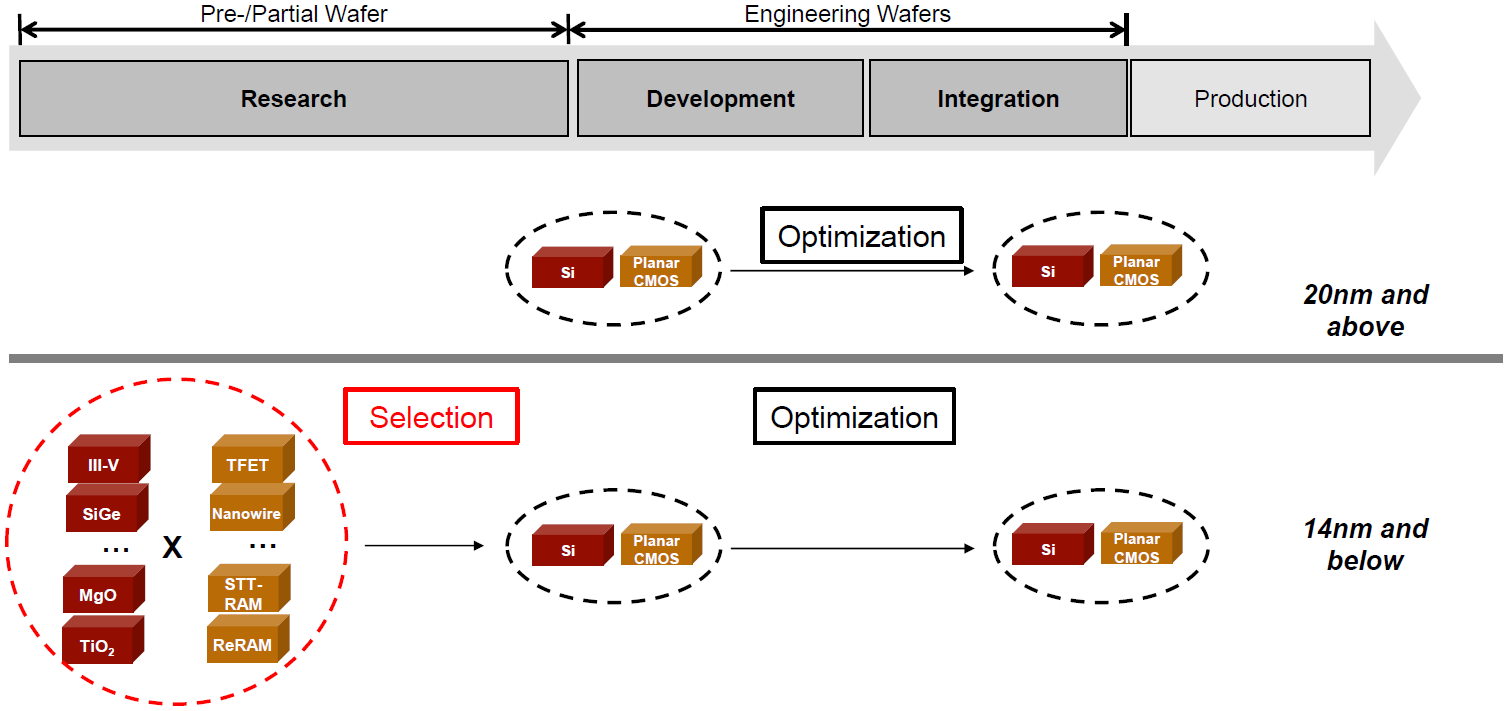
Image courtesy Synopsys
Called “ab initio,” or “first principles,” (literally, “from the beginning”) tools, they offer the least possible abstraction: they start from basic physics. They’re usually used by research department in universities or consortia, and there hasn’t really been a clean hand-off from them to TCAD.
And that’s what Synopsys is changing. To be clear, they’re not coming out with their own new ab initio tools; they’re providing an interface to the existing tools so that the results can be imported for further work.
Talking to ab initio tools is one of the critical ingredients to waferless TCAD, but it’s not enough. At the other end of the TCAD pipeline is the PDK, including SPICE models and design rules. This is where you traditionally need the wafer data. Yeah, you can get early versions of the models and rules, but the goal is to improve the quality of the early PDK so that designers can start creating circuits earlier.
In order for that to happen, the tools have to be able to simulate the entire process in order to evaluate the impact of the many different parameters influencing not just individual device performance, but also overall yield.
Being able to perform simulation both reduces and increases the number of “experiments” you might run as compared to building wafers. When doing actual wafer runs, you have to do a careful design of experiments in order to pull out all of the data you need with a minimum of wafers and pattern variants. But Synopsys notes that simulation provides much more visibility into internal variables and state, making it easier to do a simulation that may confound, or blend, various measurements and then tease them apart afterwards. This makes for fewer runs.
At the same time, however, simulation lets you play with vast numbers of variations that you’d never try if you actually had to build them all. Heck, some of them might not even be buildable. So that gives you more experiments to run. It’s not clear that you end up with more or fewer experiments, but what’s important is that you can exercise them without building physical wafers.
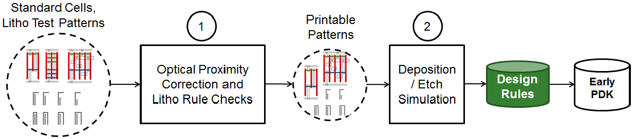
Synopsys already has a lithography simulation tool: the Sentaurus-Litho tool just mentioned. What they’ve added to the mix is a process simulator called Process Explorer. It simulates the non-litho steps like deposition and etch. Together with Sentaurus-Litho, you can take a process recipe and simulate how a wafer will be built from it. Sound familiar? Yeah, we’ll come back to that.
From a design-rule-development standpoint, you can now take a variety of patterns, see first which ones are printable, and, from those, evaluate which ones work and yield. From that data emerge design rules. Printability assessment (without wafers) has been possible for the last few years, but Process Explorer provides a faster way to simulate the other basic steps, operating about 1000 times faster than their full-on Sentaurus simulation tool.
Meanwhile, from the I-V curves that Sentaurus can create, Synopsys can use technology that they acquired from GSS to derive SPICE models for the early PDK. Early, more accurate design rules; early, more accurate SPICE models. All make for a better early PDK.
Coventor goes electrical
Meanwhile, Coventor has now added the logical next step to their process simulator: moving from the structures that they (virtually) build to the resulting electrical calculations – heretofore the realm of TCAD. Their focus is RC extraction at the moment, with other electrical influences accessed via interfaces to other solvers (although they could decide to take on more themselves in the future).
Here again, the goal is to improve the quality of early PDKs. And again, the value is in simulating wafers that you don’t have to build. They said that they “built” 1.3 million wafers in a few weeks for Imec as part of their 7-nm development exploration. You can’t build one wafer in a few weeks, so doing millions is an enormous time saver, allowing you to experiment with process variation and its effects on yield and performance.
There is still some contrast with traditional TCAD, even given what Synopsys has recently announced. TCAD focuses on a single device, while Coventor has worked with larger circuits and cells. TCAD looks for fundamental device characteristics; Coventor looks at manufacturability. That hasn’t really changed, but the lines are now definitely much blurrier than they used to be.
I asked each company for comment about the fact that there appeared to be some mutual encroachment here, and there’s definitely mutual awareness.
Synopsys describes Process Explorer and SEMulator3D as being quite similar, but they use the term “process emulation” rather than “process simulation.” Their distinction is that time savings are gained by not modeling all of the process steps like doping and thermal operations (annealing etc.). They contend that, to get the full value out of the process emulator, you need to be able to hook it to a variety of other simulation tools – like Sentaurus – so that you can further refine the work that the process emulator has done.
Coventor says that they understand the basic notion of process emulation and that they can run SEMulator3D in that mode – but that it’s only one of several modes that allow their users to dial up or down the detail (and run time) they want. They say they can do full process simulation and are not limited simply to deposition and etch.
Also, while Synopsys deals with lithography in a separate tool (Sentaurus-Litho), Coventor says they can handle that within SEMulator3D – or, as an option, they can import optical corrections and such from an external tool.
My conclusion is that the edges of these galaxies are touching. Not clear yet whether the larger galaxy is feeling “poked” by the smaller one, but the cosmic pas de deux has definitely been engaged.
More info:
Synopsys Silicon Engineering tools


Do you see Synopsys and Coventor going head-to-head on tools that allow more process development with less wafer building?
Coventor’s tool is not a process simulator in the TCAD sense. They themselves have referred to SEMulator3D as a process emulation tool.
http://www.coventor.com/blog/process-simulation-vs-process-emulation-is-semulator3d-really-tcad/
Coventor had a TCAD link through GSS, but then Synopsys bought Gold Standard Simulations out.
http://www.coventor.com/blog/linking-virtual-wafer-fabrication-modeling-with-device-level-tcad-simulation/