

As we continue to try (and succeed at) stuffing more circuity into a tiny space than physics allows without great cleverness, we are drifting more and more into the use of multiple patterning. We’ve looked at this a number of times, starting with the simplistic view of litho-etch-litho-etch (LELE) approach and then digging deep into the far less intuitive self-aligned (or spacer-assisted) double-patterning (SADP).
As we’ve mentioned here and there, these technologies are, to some extent, in production – and more is coming. What’s a bit confusing is what’s coming when and why. Today’s musings attempt to sort that out.
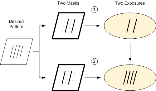
But before we do that, let’s do a quick review (with more details available in the prior pieces linked above). Multiple patterning is a trick we play so that we can place features closer together than can be done with a single exposure. The solution? Split the mask pattern in half and do two exposures.
Basic double-patterning (LELE)
The trick is in the splitting of the mask: each mask has only some of the features and has to obey rules for a single exposure; overlaid on top of each other, you end up with all the features, and, if you played your cards right, it looks as if you did it all with a single mask. The big physical challenge is overlay, of course – making sure that the second exposure lies directly atop the first exposure.
And from a simulation standpoint, Mentor says that you can’t treat the combined lines as if they were done at once: Capacitances and impedances in metal lines, for instance, my vary slightly between exposures due to slight mis-registrations, adding a complicating factor to low-level circuit modeling.
Although this double- (or triple- or quadruple-) patterning concept is straightforward, we have ended up with the two basic flavors mentioned above: LELE (which is LELELE for triple patterning, etc.) and SADP (which is SAQP for quad-patterning). With LELE, you literally split the layout in half (following careful “coloring” rules to ensure that each half follows layout rules). With SADP, it’s a much more convoluted process resulting in masks that look little like the features being created on silicon. This is what we dug into deeply in the second article linked above, and I’m not going to repeat the craziness here.
But what’s less clear is where these different technologies are going to be used. In a lithography discussion earlier this year, I reported some comments from Applied Materials’ Chris Bencher regarding usage, and he spoke of the success to date of SADP and even SAQP.
In a DAC discussion with Mentor, however, the picture was described very differently, with LELE dominating at present and SADP waiting in the wings. So I wanted to try to reconcile those two views – and, in so doing, I also tripped over yet another variant in this whole thing, which we’ll get to shortly.
In bringing these two views together, it’s helpful to note that Applied Materials is a semiconductor equipment manufacturer and is therefore about as close to the silicon as you can get. Mentor is an electronic design automation (EDA) company, and, while they still need to be pretty close to silicon to be sure that their models and simulation have good fidelity, by definition, the abstraction they provide represents a slight removal from the silicon.
Which brings us to two distinct camps of designers. Actually, there are three including analog, but we’ll let those guys rest on the sidelines for the moment, since analog layouts aren’t the ones pushing the limits. No, these two groups we’ll discuss both consist of digital designers. The difference is, one group does custom design – memories, FPGAs, things like that. And they do their designs by hand, meticulously.
That works largely because these are highly repetitive designs, meaning that extended tender loving care can be lavished on the cell, which is then replicated wildly onto the chip. They make much less use of EDA tools, which, by contrast, are used extensively by logic designers when fashioning systems-on-a-chip (SoCs).
Memories tend to lead new density-enhancing trends, so it’s entirely likely that Applied Materials and other equipment guys would be affected before Mentor and the other EDA folks would. That said, everyone has been working on it; Mentor says that its basic “coloring engines” are ready and simply waiting for rollout.
In fact, Mr. Bencher says that NAND Flash has been using SADP for five generations, with some manufacturers now moving into pilot SAQP production. DRAM also has a couple of nodes SADP under its belt. These are both high-volume technologies, meaning that, even though few designers have had to deal with the complications, it’s got the lead in volume at this point.
With logic, things have taken a different route. At 20 and 16/14 nodes, LELE is the dominant approach. Even so, things are more complicated than that. In order to make sense out of what’s going on, there are really five different kinds of mask that we need to consider:
- Fins: this is for creating the FinFET channel. Notable is the fact that all widths are the same.
- Metal lines: these have reasonably random routes these days, but at some point (10-nm?) they will be required to be 1D – that is, go only in the x direction or the y direction; no corners or jogs. Unlike fins, widths may vary.
- Contacts: exceedingly small holes through dielectric through which the silicon is accessed.
- Vias: still pretty danged small holes allowing contact between metal layers.
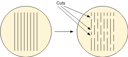
- Cuts: once 1D metal rules are in place, then metal features will be defined by two steps: laying down the lines and then cutting them to define the 1D features.
At 20/16/14 nm, you don’t really have a line/cut methodology; it’s just metal, and the metal and contacts are done using LELE. But it turns out that the fins are done using SADP. The catch (or perhaps the saving grace) is that creating the required masks is done by the foundry, meaning that designers are protected from having to think in SADP terms.
LELE also requires coloring, but (a) it’s much more intuitive and (b) for now, it’s also generally done by the foundries. So… logic designers have had it easy so far.
One other consideration is the fact that fins all have the same width. You may recall that SADP has some restrictions when it comes to the widths of the features it can create. Fins work well with that; metal lines that may need arbitrary widths, not so much. Which is consistent with the current use of SADP for fins and LELE for metal.
At 10 nm, metal is likely to move to SADP. But it’s actually a reverse or negative version of the SADP being used for fins. Yes, just when you thought it couldn’t get any more confusing, we have two flavors of SADP. The first one, and the one we’ve covered in detail, is called “spacer is mask” or “SIM” – in other words, the spacers that are created define the mask features. But for metal, rather than defining the metal lines, it will define the spaces between the lines, which is dielectric material – hence the name “spacer is dielectric,” or SID. As far as I can tell, that should mean that the SADP width restrictions will apply to the dielectric, not the metal.
So while SIM SADP will continue for fins, the 10-nm node should see the start of SID SADP for metal. Metal 1 may also go to 1D rules at this point. What’s notable here is that the designer will need to be involved in the SID mask decomposition process, at the very least labeling mandrel features and non-mandrel features. Software will still do much of the detail beyond that, but it’s unlikely to be completely transparent to the designer.
Mentor’s David Abercrombie also sees some foundries possibly opting for triple-patterning – LELELE at 10 nm, instead of (or, perhaps if the choice is made layer-by-layer, in addition to) SID SADP for the metal lines.
With contacts at 10 nm, Mr. Bencher sees them moving to SADP; Mr. Abercrombie saw folks moving to LELELE, with some folks moving all the way to quad-patterning – LELELELE. Vias will remain LELE.
So let’s try to summarize here:
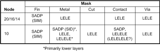
Where there are options, then which one gets used for any specific design will depend on the design and feature density, metal layer, and foundry being used.
Having hashed through that, it’s almost comical to think back about four years when I first wrote about this. It seemed so simple then, and now it’s fragmented into all of these variations for different purposes. But each flavor has its plusses and minuses, and, above all, you want to stay with the simplest solution possible. Which means that more complicated approaches will be used only selectively, when absolutely needed, which leads us to this complicated matrix.
Not even gonna think about 7 nm at this point…


How do you see multi-patterning rolling out? Do you have additions to the table?