


I love surprises like this. You go into what promises to be a wonky, even dull, conference presentation – and come out agog.
That’s exactly what happened to me at the recent ICCAD in San Jose. It was a presentation based on a collaboration between the University of Michigan, Shanghai Jiao Tong University, and National Tsing Hua University about some placement or routing algorithm, but it happened to involve a transistor type that I’d never heard of. And… I don’t know, there was something about the regularity of it, perhaps its elegance, illuminated through a very lucid presentation, that caught my fancy. Heck, even with no prior knowledge, I could actually follow most of the talk. That was exciting enough. Great success!
So… what was this thing? It was a way of implementing logic on a fabric of single-electron transistors (SETs). In fact, a reconfigurable fabric. This could be your new FPGA some years hence. But, while I could follow the logic of the presentation, I had no idea what a SET was, nor did I understand why certain constraints existed that affected the algorithms presented.
So, having plowed through the interwebs for more information, I decided to split this story into two. First we’ll discuss the underlying semiconductor technology. That will pave the way for a discussion of the EDA implications in a separate article to be published shortly. There are a fair number of places from which to piece together information on some of these concepts, but I found two papers particularly illustrative. One is the ICCAD paper just mentioned; the other is a paper from Penn State on the actual fabric. Links to both follow at the bottom.
A Quantum of Current
First off, we’re talking about a tiny transistor featuring the tiniest of currents. Great for ultra-low power and low voltages, but it puts us into the weird, spooky world of quantum. In particular, we’re dealing with a current that’s as low as physically possible – so low that it’s quantized.
How could it be quantized? Because you can’t get a lower current than moving a single electron. This is done through a tunnel barrier and involves a phenomenon called “Coulomb blocking.” As I was reading about it, it struck me as surprisingly familiar – there are ways in which it brings Fowler-Nordheim tunneling (of EEPROM fame) to mind.
The idea is to isolate a quantum dot. A quantum dot is a zero-dimensional “point” – having lost a dimension from the one-dimensional quantum wire, which loses a dimension from the 2-D quantum well, which itself is a dimension short of 3-D bulk material in which quantization goes away.
The dot is, of course, of finite dimensions; it’s not an actual infinitesimal point. But it’s constricted enough to limit severely the number of states available for hosting electrons. By applying a potential, you can move a single electron over into an unoccupied state that’s at a lower energy (thanks to the applied voltage).
But once that electron moves, the state is full (assuming the potential made only one such state available). Looked at differently, the electron now opposes the applied potential, so a yet higher potential is needed to move yet another electron. This self-limiting nature was specifically what reminded me of Fowler-Nordheim tunneling, where the accumulating electrons on a floating gate oppose the voltage that got them there. Kind of like folks moving into a new neighborhood and then trying to pass ordinances making it hard for others to move in.
SETs are built using quantum wires (also called nanowires); no ordinary wires these, they have quantized conductance due to the confinement of the wire. More on how these are arranged in a minute. For now, let’s concentrate on the transistor itself.
Tunneling Transistors
A SET looks a lot like an MOS transistor. It consists of a drain, an “island,” and a source, all separated by tunnel barriers. Control is provided by a gate – no current tunnels to or from the gate.
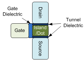
That island is the quantum dot, and the gate controls the potentials that allow or disallow current. I’m not going to get into the details of how this works because it immediately dives into the infernal world of quantum wave functions, which are nice and all, but they suck all the life from quantum – at least for me. OK, ok, you need the math to do anything useful, but this isn’t a how-to, so we’re moving on.
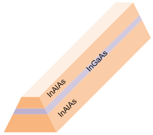
The way this transistor is implemented starts with the concept of the wrapped-gate nanowire; let’s address the nanowire part of that first. A nanowire isn’t simply a small wire; it needs proper confinement. These guys built that by creating a “heterostructure” consisting of an InGaAs layer sandwiched between two InAlAs layers. The middle layer is the conductor, and the layers above and below it provide the confinement to one dimension. The “pyramidal” (sort of) cross section of the wire comes about due to crystal orientation; a bit more on that later.
A further step is then taken to provide the one more element of confinement needed to get a zero-dimensional quantum dot. This is done using “wrapped” gates – two of them, between which a dot can be formed. In the simplest implementation, both gates originate as a “split” from a single gate signal.
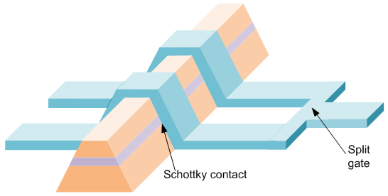
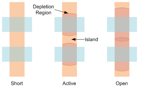
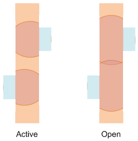
These wrapped gates aren’t the “gate” shown in the first drawing: they’re a means of taking a nanowire and creating – or removing – a quantum dot (we’ll get to the other gate – the “control gate” – in a minute). As originally implemented, each gate wraps three sides of the nanowire. By adjusting the potential on the gate, you create depletion regions by virtue of a Schottky contact with the nanowire, and the extent of those regions defines how this operates.
With a high voltage, no depletion region exists, and the nanowire acts like… a nanowire. If you apply a very negative potential, two depletion regions will form and overlap, blocking all conduction. Somewhere between those extremes, the depletion regions will create limited barriers, with a space between them. The regions themselves are then the tunnel barriers, and the space between is the quantum dot. In this state, the transistor is said to be “active.” This literally means that, during operation, transistors can be created or removed in real time.
The control gate – this is the gate that acts like the MOSFET gate – is then added on the top. So you have the two wrapped gates in close contact with – and therefore with strong influence on– the nanowire, and you have the control gate that also has strong influence (although slightly less so) by virtue of a high-? dielectric.
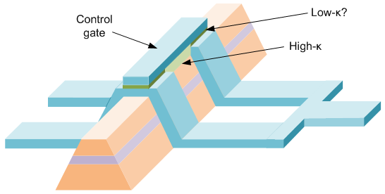
In the image above, I’ve made an assumption, since there are only so many of the fabrication details that I’m aware of, and I don’t want to get completely lost in minutiae. But, just as you’d want high-? for coupling the control gate to the quantum dot, so you’d want to make sure the control gate doesn’t couple to the wrapped gates. As shown (which is similar to a drawing in the paper), that would suggest a low-? material there. I could be wrong… but then again, this is but a way-station. We’re not stopping with this configuration.
A Non-Volatile Device
So far so good. But the Penn State folks have taken things one step further. Rather than splitting a single gate, they’ve made the lines independent. They did this by removing the full wrap, relying entirely on one sidewall for contact. They claim this as a critical part of their proposed structure. (Note that the low-? question is now moot.)
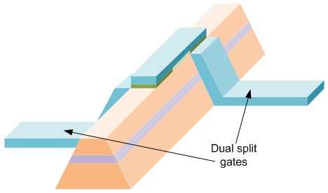
Note that the depletion regions would now emanate from one side only. Presumably this would have some effect on the actual potentials used for the active and open states.
They’ve then added non-volatile storage. One way of doing this is to use a ferro-electric material – analogous to a magnet that can be repolarized, except that it’s an electric dipole rather than a magnetic one. You may be familiar with them as used in FRAMs. It’s inserted between the now-unwrapped gate and the nanowire.
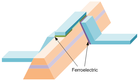
This material now forms the Schottky contact; the erstwhile wrapped gate no longer touches the nanowire directly.
This means that the wrapped gate lines, rather than being real-time arbiters of the transistor configuration, now become part of the programming infrastructure, and a non-volatile cell is programmed to create (or not) the depletion regions that determine how the device operates.
Here again there are details I’m not sure about. Like how such a material would be deposited, and whether the way I’ve drawn it would reflect an “as-built” configuration. It may be a conceptual view only, or perhaps a configuration for small-scale labs. But it should serve our purpose for the nonce.
I think it’s worth pausing a moment to reflect on this: if this all works as advertised, then you can create a fabric out of this stuff and program it to implement any logic. How that works, we’re coming to next. But you’ll notice that this involves no SRAM bits for storing state, there’s no external non-volatile memory keeping track of things while we’re powered down. A “simple” layer of non-volatile storage material sandwiched in there lets us set and maintain the configuration whether powered up or not. Of course, it takes some infrastructure to do the programming… we’ll come back to that.
All details aside, this seems pretty cool to your intrepid reporter.
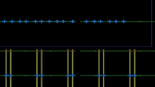
A Hexagonal Fabric
Let’s move on to how we connect these things to do something useful. This isn’t going to be your usual configuration of gates driving other gates: there simply isn’t enough drive current to do that. So a completely different approach is used.
Other work (also linked below) shows how you can use selective etching to create a hexagonal array of nanowires. The selectivity comes along crystal boundaries, and it drives the hexagonal angles in the horizontal plane. It also gives the pyramidal structure of the nanowires. That particular paper uses GaAs sandwiched between AlGaAs, but the concept is similar to the version we described above.
The way such a hexagonal array works is as follows:
- Each “vertical” line remains a short; it has no SET.
- The angled lines are outfitted with the gates necessary to make a SET.
- Along each horizontal row of angled lines, crossing all hexagons, one variable drives all the control gates (a and b and the dashed lines in the drawing below).
- From each vertical line, you get an angled line going down to the left and one going down and to the right. One represents the “true” version of the control variable for that SET; the other represents the complement (or “false” version). Which is which is something we’ll come back to; one implementation is shown below.
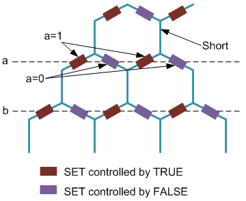
This figure uses a particular arrangement where the line coming down and to the left represents the true value of the control variable; the line coming down to the right side represents the false value. The way we perform logic is to have a “top” of this network where we “insert” current (even though the electrons are actually inserted from the bottom) and then configure these SETs to pass or block the current according to the control variables.
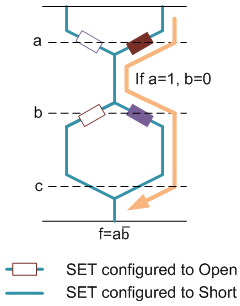
This is where the programming of the SETs is critical. If a logic function needs the negative value of a variable, then the corresponding active low SET is programmed to the active state – and the SET on the active high side is programmed to block current.
The following figure shows the simple example implementing the function “f=ab?” in a fabric having control gates for variables a, b, and c. Variable c doesn’t figure into this function, so those SETs could be configured as shorts (for simplicity in this view). The SETs for the unused polarities of a and b are configured as opens; they never conduct. So the only way current can flow is when a is 1 and b is 0 (using active high logic). The practical assumption is that there is a current detector at the bottom or top that will determine whether or not a current has passed.
Because these networks get complicated for more serious logic, some notational shortcuts have been adopted, so you’ll mostly see networks that would make the function above look as follows:
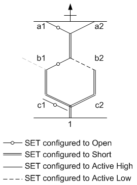
Note the different line characteristics as well as the fact that each node is labeled with its variable. a1 and a2 both represent variable a, and they can’t take on different values of a, but they represent two different decision points. This becomes more useful for EDA algorithms assigning logic to nodes.
Note also that in the case of node c1, I’ve shown it as short, but, as indicated, it could also be open. If other nodes from b came in from the left (the gray dashed line), for example, then you’d probably want to cut off that path so that it didn’t represent a sneak path that messed up the evaluation of the function involving only a and b. (Then again, that dashed line could also be configured as an open, blocking current there…)
Spoiler alert for the next article: this arrangement looks strikingly similar to a binary decision diagram (BDD). That’s no accident. More about that in the EDA follow-up, when we’ll make yet more simplifications to the fabric drawings.
Fabrics and Constraints
Ok, we’re almost there. Two important considerations remain. First, I mentioned the question of whether the active high or low states branch to the left or right. That’s a fabric design decision. What we show in the above figures has active high going to the left and active low going to the right; this is referred to as a “symmetric” fabric. But it doesn’t have to be that way.
A “mirror” fabric would reverse the directions at every node. Then there are “sparse” fabrics that are mostly one way, with the occasional reversal.
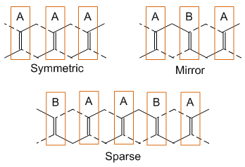
Why these options? Because optimizations sometimes make it useful to share “sub-trees” – parts of the logic useable in common by different functions. Depending on whether these sub-trees are desired in their true or complement form affects how you’d like the fabric to look. There’s no one right answer for every situation.
This question gives rise to a “fabric constraint” that must be met by the placement algorithms. The exact nature of the constraint depends on the organization of the fabric. We’ll see that in action in the follow-up piece.
Finally, there’s the issue of programming infrastructure. A grid of vertical and horizontal wires is needed for x/y addressing to program individual SETs. That gets to be a lot of wires, and so some sharing has been proposed to cut down on the congestion. You could share one wire for two neighboring nodes or for four (or more). The more sharing, the more constraint you place on what can be placed where, since you’ve reduced some degrees of freedom; you can no longer program each node independently of other nodes.
This gives rise to what’s called a “granularity constraint.” The granularity in this case refers to how many nodes are interrelated in this way. The most granular arrangement is for each node to be independent; these optimizations reduce the granularity, and they affect how logic is to be assigned. Again, we’ll see this put to effect in the next article.
OK…That’s it for now. From a collection of a number of simple concepts we get this fabric that’s strikingly simple and seems relatively efficient. Then again, we’re looking at it only from a conceptual standpoint. This isn’t necessarily an ivory-tower exercise, since some of the manufacturing considerations have been studied. But we’ve pretty much ignored manufacturing, and there are probably potential issues that are not even known yet. So in case it’s not obvious, this is still a research topic.
There is one clear limitation in what we’ve seen: this is purely a combinatorial fabric. There’s no intrinsic way to route feedback for flip-flops (nor was any raised in the papers I’ve read). Presumably such a modification would involve taking the results from the detectors and routing them to variables (the horizontal lines controlling the control gates). Let’s leave that as an exercise to be sorted out by the researchers.
Next up: how you take logic and implement it on this fabric. Which was the topic of the ICCAD paper that started this whole thing. We just couldn’t get there without first addressing the basics.
More info:
Reconfigurable BDD-Based Quantum Circuits
BDD-based synthesis of reconfigurable single-electron transistor arrays (behind paywall)
Hexagonal fabric: I have a paper that I can no longer find except behind paywalls. If you search, you may also find an open copy. Here is an open abstract of the work: https://www.electrochem.org/dl/ma/206/pdfs/1039.pdf
Formation of High-Density GaAs Hexagonal Nano-wire Networks by Selective MBE Growth on Pre-patterned (001) Substrates (behind paywall)


Are single-electron transistors what our future will look like?