

Last December’s IEDM conference included a couple of sessions on non-volatile memory of the phase-change type. The most familiar of these is PCM – phase-change memory – where a substance is either melted and quenched before it can crystalize, leaving it in an amorphous state, or is allowed to solidify in an orderly, crystalline fashion. The resting state of the material – amorphous or crystalline – determines the resistivity, and hence the value, of the bit.
PCM has been a promising new technology for a long time now, and there will be more to say on that in a minute. But it also has a weakness: you need enough energy to melt the bit. Well, there’s a new way of attempting something like this with less energy: “topological switching RAM,” or TRAM. The “phases” between which it switches are more subtle than amorphous vs. crystalline.
TRAM uses a “superlattice” of GeTe and Sb2Te3. A superlattice is a crystal-like lattice consisting of alternating rows of two materials. Looking at their figure, it would seem that there are two atomic layers of each material in alternation. The trick here is that the Ge has some flexibility in terms of how it is arranged with respect to its Te counterpart. The two states consist of one where the Ge gets between the Te atoms in adjacent GeTe layers; the other state has Ge on the other side of its Te partner, meaning that the Te of the two layers are next to each other.
In that latter state, there’s effectively a small channel through which electrons can more easily flow, so this is a low-resistance state. With the Ge atoms in the way, resistance is higher.
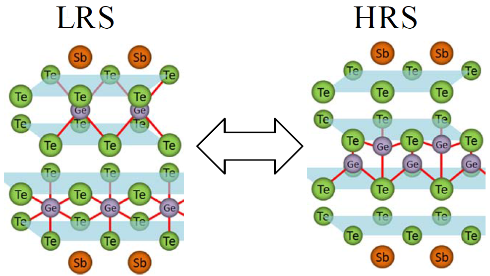
Figure 1. The two TRAM states: low resistance (LRS) and high resistance (HRS) (Image courtesy IEDM)
It potentially takes less energy to move the Ge atoms around than it would to melt a bit in a PCM. But exactly how easily the Ge moves depends on the vacancies and the share of Ge. The reporting team, from the Low-power Electronics Association & Project; the Graduate School of Pure and Applied Sciences, University of Tsukuba; the Graduate School of Engineering, Nagoya University; and the National Institution of Advanced Industrial Science and Technology, all in Japan, played with the proportion of Ge to find the optimal level.
They found that, given a compound GexTe1-x, if x>> 0.5 (x=0.5 is GeTe), there wasn’t enough mobility for the Ge to move about. If x<<0.5, the switching energy was lower than with GeTe. In other words, it’s best to “dope” the Te lightly with Ge, leaving it plenty of room to move.
The cell they came up with could be programmed with 55 µA of current (set or reset) and yielded a 100x resistance ratio (that is, the set resistance vs. the reset resistance). And it had an endurance of 100 million cycles.
You can read more about it in the IEDM proceedings, session 29.2.
Meanwhile, a follow-on presentation discussed the current state of PCM. PCM has been “promising” for a long time, and has been perpetually a few years away from being ready for commercial use. The presenter was quite candid about this challenge as he noted that, to date, DRAM remains faster, NAND remains cheaper, and the NOR market is shrinking.
He described possible usage in storage-class memory (kind of like a cache for hard drive data), TCAM, and “smart” memory (essentially building a synapse). And he set out 2018 as a date when this could be ready.
He gets credit, however, for the most honest answer I think I’ve ever heard at a conference, when asked by an audience member, “Why use PCM for those applications instead of ReRAM or STT memory?” His answer was, “Because I’m working on PCM, not ReRAM or STT.”
I honestly have to say that I was left with the impression that PCM’s days are behind us.
You can find this paper in the IEDM proceedings, session 29.3.


