

Cadence is a pivotal leader in electronic design, building upon more than 30 years of computational software expertise. The company applies its underlying Intelligent System Design strategy to deliver software, hardware and IP that turn design concepts into reality.
Cadence Blog – Latest Posts

Cadence to Power the Fourth Industrial Revolution in Collaboration with NVIDIA
The convergence of artificial intelligence (AI), robotics, and the internet of things (IoT) has brought about the fourth industrial revolution. It's reshaping how we design, manufacture, and interact with the world. At the heart of this era lies a powerful catalyst: arti...

Cadence San Jose Hosts JEDEC LPDDR Task Group Meeting
Low-power DDR ( LPDDR ) SDRAM has been one of the most widely used memories in the semiconductor market today. It’s used in a diverse set of applications that spans mobile/handheld devices, IoT, client and server, automotive, Virtual Reality/gaming consoles, robotics, data ...

Custom Analog IP Migration in Virtuoso Studio
Join Cadence Training and presenters from our CIC experts for this free technical Training Webinar. The porting of a custom IP block to a new silicon process has traditionally been a manual process. However, the introduction of new algorithms in Cadence’s Virtuoso Studio,...

Efficient Automotive Electronic Component Design and Analysis
In the automotive industry, there is zero tolerance for field failures, as human safety is at stake. Given the rapid evolution of the electric vehicle (EV) and autonomous driving technologies, it is critical to accelerate the development of robust designs to remain competitiv...

NOP Flit Payload: A Dedicated Debug Channel
Modern PCIe systems are complex, with high-speed data transfer and intricate protocols. Traditional debug methods often struggle to provide the necessary granularity and real-time visibility into link behavior. Transient issues, timing-sensitive errors, and protocol interacti...

Silicon Skylines: Crafting the Future of Electronics
The world of Electronic Design Automation (EDA) is fascinating, where we transform humble grains of sand into sophisticated silicon chips that power our modern lives. Imagine this journey as a grand adventure, akin to building a bustling city from scratch. Buckle up as we tak...

Cadence 率先推出 eUSB2V2 IP 解决方案,助力打造高速连接新范式
为了提供更好的用户体验,包括高质量的视频传输、更新的笔记本电脑(例如最新的 AI PC)和其他前沿设备,都需要 5 纳米及以下的先进节点 SoC,以达成出色的功耗、性能和面积(PPA)目标。然而,随着技术�...

NepTech – Tackling Marine Decarbonization with Fidelity CFD
Maritime transport is the backbone of international trade. It’s responsible for transporting over 80% of global goods, making it critical for commerce and trade. At the same time, it’s the world’s sixth-largest emitter of greenhouse gases. Now more than ever, maritime d...
Chalk Talks Featuring Cadence
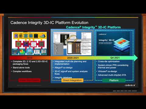
Faster, More Predictable Path to Multi-Chiplet Design Closure
The challenges for 3D IC design are greater than standard chip design - but they are not insurmountable. In this episode of Chalk Talk, Amelia Dalton chats with Vinay Patwardhan from Cadence Design Systems about the variety of challenges faced by 3D IC designers today and how Cadence’s integrated, high-capacity Integrity 3D IC Platform, with its 3D design planning and implementation cockpit, flow manager and co-design capabilities will not only help you with your next 3D IC design.
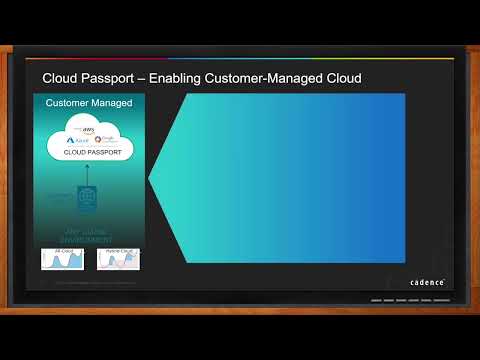
Enabling Digital Transformation in Electronic Design with Cadence Cloud
With increasing design sizes, complexity of advanced nodes, and faster time to market requirements - design teams are looking for scalability, simplicity, flexibility and agility. In today’s Chalk Talk, Amelia Dalton chats with Mahesh Turaga about the details of Cadence’s end to end cloud portfolio, how you can extend your on-prem environment with the push of a button with Cadence’s new hybrid cloud and Cadence’s Cloud solutions you can help you from design creation to systems design and more.

Machine-Learning Optimized Chip Design -- Cadence Design Systems
New applications and technology are driving demand for even more compute and functionality in the devices we use every day. System on chip (SoC) designs are quickly migrating to new process nodes, and rapidly growing in size and complexity. In this episode of Chalk Talk, Amelia Dalton chats with Rod Metcalfe about how machine learning combined with distributed computing offers new capabilities to automate and scale RTL to GDS chip implementation flows, enabling design teams to support more, and increasingly complex, SoC projects.
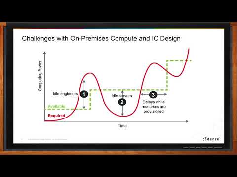
Cloud Computing for Electronic Design (Are We There Yet?)
When your project is at crunch time, a shortage of server capacity can bring your schedule to a crawl. But, the rest of the year, having a bunch of extra servers sitting around idle can be extremely expensive. Cloud-based EDA lets you have exactly the compute resources you need, when you need them. In this episode of Chalk Talk, Amelia Dalton chats with Craig Johnson of Cadence Design Systems about Cadence’s cloud-based EDA solutions.
Featured Content from Cadence
featured video

How Switch Provides Unparalleled Exascale Data Center Solutions with Cadence and NVIDIA
Learn how Switch, a leading designer, builder, and operator of U.S. exascale data centers, is taking their data center’s cooling capabilities even further. In the past 20 years, Switch has built some of the densest air-cooled data center environments. With AI taking off in the last couple of years, see how they were able to deploy many of the first NVIDIA H100 clusters inside using Cadence’s Reality Digital Twin Platform for pre-modeling, design, and validation.facilities.
featured video

How NV5, NVIDIA, and Cadence Collaboration Optimizes Data Center Efficiency, Performance, and Reliability
Deploying data centers with AI high-density workloads and ensuring they are capable for anticipated power trends requires insight. Creating a digital twin using the Cadence Reality Digital Twin Platform helped plan the deployment of current workloads and future-proof the investment. Learn about the collaboration between NV5, NVIDIA, and Cadence to optimize data center efficiency, performance, and reliability.
featured video

Larsen & Toubro Builds Data Centers with Effective Cooling Using Cadence Reality DC Design
Larsen & Toubro built the world’s largest FIFA stadium in Qatar, the world’s tallest statue, and one of the world’s most sophisticated cricket stadiums. Their latest business venture? Designing data centers. Since IT equipment in data centers generates a lot of heat, it’s important to have an efficient and effective cooling system. Learn why, Larsen & Toubro use Cadence Reality DC Design Software for simulation and analysis of the cooling system.
featured video

Why Wiwynn Energy-Optimized Data Center IT Solutions Use Cadence Optimality Explorer
In the AI era, as the signal-data rate increases, the signal integrity challenges in server designs also increase. Wiwynn provides hyperscale data centers with innovative cloud IT infrastructure, bringing the best total cost of ownership (TCO), energy, and energy-itemized IT solutions from the cloud to the edge.