editor's blog archive
Subscribe Now

A HEMT Cool-Down

Heat has got to be one of the most annoying side-effects of doing useful electrical work. The more work we do, the more things heat up, changing the characteristics of the circuitry and, if we’re not careful, leading to early end-of-life or outright failure.

It’s heat that’s part of why we’ve gone to multicore instead of simply ratcheting up microprocessor clock frequencies forever. Greater dissipation is one reason we end up with power transistors that are larger than they need to be for electrical reasons. And when 3D ICs … Read More → "A HEMT Cool-Down"

In-Situ Real-Time Process Checks

Yesterday we looked at number of different ways of inspecting wafers. Such inspections can be an important part of a process that turns out high yields of high-quality chips. They serve a couple of roles in this regard.

The most obvious is that you catch faulty material early. If rework is possible, you can then rework it; if not, well, you don’t throw good processing money after bad.

But the other reason is probably more important: by looking at … Read More → "In-Situ Real-Time Process Checks"

A New IoT Protocol

We’ve got a number of ways of getting our devices to talk to each other. Some time back, I opined that Bluetooth Low Energy and WiFi seemed to have the edge, largely influenced by the burgeoning Internet of Things (IoT). Zigbee, meanwhile, seems to have more sway in the Smart Grid.

Well, some folks still aren’t happy with these options. There are three capabilities that are … Read More → "A New IoT Protocol"

A PIC for the IoT

If you’re building a Thing for the Things’ Internet (consumer-edition – i.e., the CIoT), then, even though you may do your heavy computing work in the Cloud, you’ll still need something to make your thing act more intelligent than the assembly of metal and plastic that it is.

Perhaps you’ll need it for management, perhaps for sensor fusion; it’s not likely to be a difficult computing challenge, but you’ll need something. … Read More → "A PIC for the IoT"

First Formal DDS Security

As noted in today’s article on some of the characteristics of the DDS data transport standard, it’s missing a rather important component: formalized security. Proprietary schemes have been layered on top of it, but the OMG has a beta standard that they’re now finalizing (a process that could take up to a year).

But that doesn’t stop early adoption. RTI has announced an implementation of the new OMG security standard for DDS – something likely made easier since, … Read More → "First Formal DDS Security"

Hello everyone, Paul Karazuba fr

Hello everyone, Paul Karazuba from QuickLogic here.

Just a few clarifications – while we are definitely less than 250µW active power for our wearable specific sensor hub designs, I think it’s only fair to point out that our ArcticLink 3 S1 sensor hub is also less than 250µW active power for Smartphone-centric sensor hubs, while maintaining KitKat compatibility.

Also, regarding Rich’s comment, I suppose this all depends on what you are trying to do — if you strapped your wearable onto a drone and are using it to control the drone, then a high data rate … Read More → "Hello everyone, Paul Karazuba fr"

Anything But Moore’s Law

Novati_fab.jpg

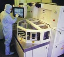
Any new foundry would want to grow up to be a megalith like TSMC, right? Isn’t that how you prove you’ve “made it”? Well, not if you’re Novati. They’re a different sort of foundry, one you don’t hear about so often over the noise of the Big Guys.

Here’s the thing: when you’re in the foundry mainstream, … Read More → "Anything But Moore’s Law"

Planning PCB, Package, and Die Together

Silicon chips and the packages that house them have been steadily drawing closer to each other over the years. There are so many pins on individual dice now – and multiple dice are going into single packages. Optimizing which bumps from which dice go to which pins is a non-trivial project.

Part of the problem is that package design and die design have traditionally belonged to different departments using completely different tools that don’t talk to each other. That’s left engineers using Excel and such to try to visualize and plan pinouts.

< … Read More → "Planning PCB, Package, and Die Together"

An Optical MEMS Reference Process

A while back Micralyne announced a MEMS reference process. There are a few of these running around: attempts to achieve – or at least grasp at – a standard process that can address a wide range of MEMS devices.

Most of Micralyne’s processes are confidential, per their customer relationships, in typical MEMS style. What they did here was to take a “neutral” improved version of what they do well and open it up. They’re not sure that customers will simply line up and use that process in high-volume production outright, but … Read More → "An Optical MEMS Reference Process"

featured blogs
Nov 22, 2024
We're providing every session and keynote from Works With 2024 on-demand. It's the only place wireless IoT developers can access hands-on training for free....
Nov 22, 2024
I just saw a video on YouTube'”it's a few very funny minutes from a show by an engineer who transitioned into being a comedian...