


ANSYS BLOG
January 21, 2021
From Chips to Ships, Solve Them All With HFSS
With the introduction of Ansys HFSS Mesh Fusion in Ansys 2021 R1, I am reminded of my amazement the first time I used HFSS more than 20 years ago. And in my opinion, HFSS Mesh Fusion is the biggest thing to happen to HFSS since HFSS. I say this because it will allow HFSS to mesh and solve far more complex designs than I ever thought possible.
I first used HFSS in 1999 for simulating Bluetooth, Wi-Fi and mobile antennas while working at an antenna startup in California. My reaction at the time was: “Where have you been all my life?” I was utterly amazed by the accuracy as well as the insight HFSS could provide.
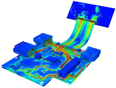
Ansys HFSS Mesh Fusion enables simulation of PCBs,
components and larger systems
Prior to HFSS, understanding how an antenna worked required time-, money- and resource-intensive measurement techniques that only provided indirect information about the electromagnetic fields. But with HFSS I was actually able to see the electromagnetic fields, to see a wave launch from an antenna. So difficult to extract in the lab, that additional electromagnetic insight accelerated our design process by leaps and bounds. And, thanks to automatic adaptive meshing, the accuracy was almost beyond belief. I remember analyzing a Bluetooth antenna’s far field pattern and plotting measured data in red and HFSS results in blue, resulting in a purple line. Subsequently, I had so much faith in HFSS, I joined Ansoft in 2001 and from there it has been a great ride with Ansys then acquiring the company in 2008.
Over the subsequent years it has been fascinating to see all the enhancements made to Ansys HFSS, such as new interfaces and new solver technologies. The market has constantly demanded bigger and faster simulation power from HFSS, and I was especially impressed by the introduction of the domain decomposition method (DDM) in 2008. DDM was a breakthrough solver technology using mesh partitioning to distribute a simulation across multiple — including networked — cores and memory to solve larger and more complex problems, allowing HFSS simulation capacity to scale up by orders of magnitude. Then in 2014 distributed memory matrix (DMM) solving delivered a matrix partitioned solver providing the low noise floor and multi-excitation efficiency of a direct matrix solver but with distributed cores and memory.
Solving Complexity Challenges with Cloud Computing
In the subsequent years, additional high-performance computing (HPC) technologies such as multi-level HPC enabled HFSS to leverage even more cores, processors and nodes. And more recently, in 2019, HFSS was enabled for Ansys Cloud on Microsoft Azure, providing HFSS users potential access to virtually unlimited compute power for solving the most complex and challenging problems. HFSS recently achieved a capacity milestone by solving an entire radio frequency integrated circuit (RFIC) front-end using the computational power of Ansys Cloud. Simulating this design with a resulting matrix size of almost 100 million was the culmination of these solver advancements leveraged on the compute resources of Ansys Cloud and demonstrates HFSS’ capacity to solve extremely large and complex designs.
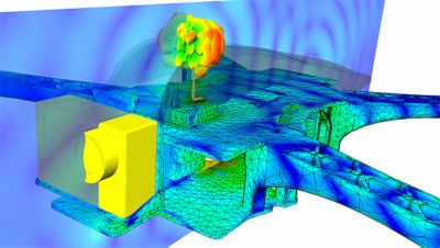
Easily mesh and plot fields of any large complex electromagnetic system
with Ansys HFSS, such as a drone with package, PCB, cables and antennas
Shorter product lifecycles, increased product functionality, and higher data rates and frequencies have constantly made delivering products to market ever more difficult for engineers. Designs have come a long way from the Bluetooth antenna that I simulated in 1999, with HFSS users analyzing designs as comprehensive as an entire 256-element 5G millimeter wave (mmWave) array antenna. An overriding drive is to use HFSS to solve more complex electromagnetic systems such as integrated circuits (ICs) in packaging, touch panel displays including capacitive sensor arrays within a housing and larger systems like multi-antenna shipboard co-site analysis.
Identifying Mesh Scaling Challenges in Simulation
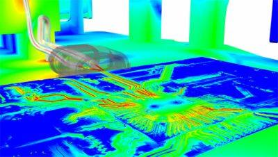
Of course, the push for bigger, better, faster always presents challenges to both meshing and solving. HFSS users are constantly pushing the envelope on what is possible to mesh and solve, such as 5G mmWave wireless modules in a tablet computer or an electromagnetic interference/compatibility (EMI/EMC) study of a complex system with multiple printed circuit boards (PCBs), including connectors and cables. Meshing is more difficult with these large-scale EM systems because the geometry is so complex with feature sizes stretching across orders of magnitude.
Ansys HFSS enables you to solve and plot fields of a complex package,
PCB, connector and cable system
The generation of a design’s initial mesh is one of the most technically challenging aspects of the finite element method (FEM) of HFSS. In generating a FEM mesh, multiple aspects of a design’s geometry come into play, such as whether it is a layered structure like a PCB; or more 3D like coaxial connectors, cables, or housing; or a platform, such as an aircraft or automobile. HFSS has multiple meshing technologies that optimally address various design types. For example, the geometry aware HFSS Phi mesher efficiently tackles layered structures found in PCB, package and IC designs, but for any given design, it has always been a one-mesh-fits-all constraint. If a design were composed of multiple “types,” for example a connector on a PCB with attached cable, achieving an initial mesh could be challenging.
Geometry scale presents yet another challenge. With today’s higher frequency content, ignoring EM coupling of an IC to its packaging can no longer be safely ignored. But in such complex EM systems, geometry detail scales from microns to millimeters presenting challenges with mesh tolerance. Creating a finite element mesh that scales up through orders of magnitude in feature size across multiple types of designs while maintaining a faithful representation of the geometry everywhere is extremely challenging and a barrier to engineering simulation.
Mesh Fusion: Multiple Meshes, Same Design, Same Reliability
To address these meshing challenges, Ansys 2021 R1 introduces a new feature: Ansys HFSS Mesh Fusion. HFSS Mesh Fusion’s patented technology enables much more complex designs to be simulated with the same rigor, accuracy and reliability of Ansys HFSS. It accomplishes this by applying targeted meshing technologies within the same design, appropriate to the local geometry.
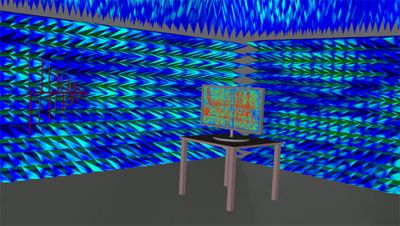
An example of simulating electromagnetic (EM) emissions from large
systems: a touchscreen TV panel in an EMI chamber.
In the previous example of a PCB with connectors and cables, the Phi meshing technology can be applied to the PCB, with the connectors and cable using the 3D-optimal TAU mesher. And there is a further virtue that the different meshing technologies can be run in parallel using HPC resources. Another advantage of HFSS Mesh Fusion is that mesh technology is applied locally with the mesh tolerance of a component defined by its size and not by the size of the overall EM system.
HFSS Mesh Fusion continues to use the same “electromagnetically aware” adaptive meshing technology as before without compromising accuracy because a fully coupled electromagnetic matrix is solved with each adaptive mesh step and for each point in a frequency sweep.
HFSS Mesh Fusion opens-up new possibilities of tackling more complex and comprehensive EM systems. Combined with the advanced elastic hardware solver technology of DMM and the option to use Ansys Cloud for hardware access — from chips to ships — there are virtually no limits to the challenges that can be solved with HFSS and the new HFSS Mesh Fusion technology.
Learn more about Ansys HFSS Mesh Fusion in this webinar.