


Are you familiar with a bird called the baya weaver (Ploceus philippinus)? These little beauties are to be found across the Indian subcontinent and Southeast Asia. Baya weavers are renowned for weaving unique and intricate hinging nests from different materials. These nests are robust and safe while also being extremely lightweight and efficient.
The reason I mention this here is that I was just chatting with Nandan Nayampally, who is the Chief Commercial Officer at Baya Systems. Just a few weeks ago as I pen these words, the folks at Baya Systems emerged from stealth mode. They picked the baya weaver as their namesake because their mission in life is to weave state-of-the-art chiplet and system-on-chip (SoC) fabrics. Baya’s software-driven IP technology portfolio is designed to accelerate both complex single-die SoC and multi-die system designs.
Nandan and I commenced our chat by considering today’s challenges, the first of which is growing complexity in silicon (single-die SoCs are complicated enough, now we are moving to chiplet-based multi-die systems), software (scaling it across heterogeneous systems), and coherency (maintaining cache coherency across chiplets and clusters). There’s also the fact that performance “guarantees” (data bandwidths, latencies, quality of service) are becoming critical across processors, memory, caches, and fabric. Then there’s the fact that costs are becoming prohibitive (silicon, power, packaging), and market windows are shrinking (faster time-to-market is required along with faster paths to scaling and to custom SKUs).
As part of this, Nandan presented the chart shown below, with which I’m very familiar. This was originally pulled together by my old chum Frank Schirrmeister. The black and yellow dots, which represent the number of transistors in CPUs and GPUs, respectively, are interesting. Also of interest are the red dots, which reflect the number of silicon IP blocks in advanced multicore SoCs. Remembering that the Y axis is logarithmic, this shows that the average number of IPs was less than ten in the late 1990s, but that it’s in the hundreds now and still rising. Also of interest is the timeline juxtaposition of the myriad AMBA protocols, including the various flavors of AXI and CHI.

Growth challenges (Source: Baya Systems)
There’s a lot of information to digest here. Sometimes it’s better to simplify things. For example, consider the upper half of the representation shown below. While simple, this depiction reflects how the performance of deep learning accelerators (red) is rocketing, GPUs (green) and CPUs (blue) are gamely trying to keep up, and memory performance—while increasing—is still managing to fall behind, with a performance gap that is growing year-by-year.

Key trends in intelligent compute (Source: Baya Systems)
In a crunchy nutshell, compute is outpacing data and bandwidth: CPU performance is outpacing memory (and the gap is widening), GPU performance is outpacing CPU performance, and dedicated deep learning accelerators are outpacing GPUs.
Meanwhile, we are in the early days of an ongoing transition to chiplet-based multi-die systems. This transition to chiplets enables best-in-class multi-vendor solutions, it will deliver advantages in terms of scale, reuse, yield, and cost in the longer term, but there is a challenge to create large, complex, chiplet-based designs in the shorter term.
Moreover, the growth of intelligent compute requires close coupling of best-in-class compute, high-performance and yet efficient data movement, and innovative complex memory hierarchy architectures.
So, how do the folks at Baya Systems intend to address all this and what do they bring to the party? I’m glad you asked. There are two main elements to this story: Weave IP and WeaverPro.
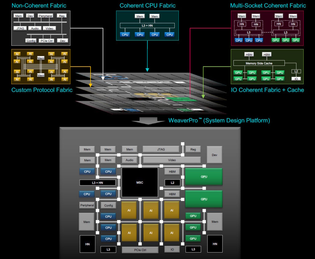
Let’s start with Weave IP, which boasts a protocol-neutral scalable custom fabric, configurable non-coherent and coherent fabrics, multi-level cache-coherent fabric, and a configurable cache controller.

Weave IP: Supported fabric protocols and functions (Source: Baya systems)
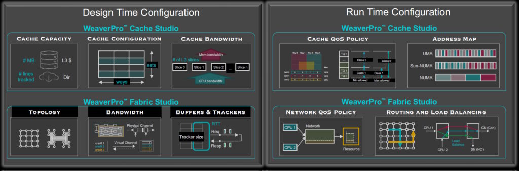
Next, we have WeaverPro, a foundational software platform that comprises two main elements: Cache Studio and Fabric Studio.
Cache Studio helps developers to rapidly design efficient memory and cache architectures, thoroughly analyze the freeform cache and memory hierarchy, simulate workloads with fast and accurate cache models, and optimize global system architecture and chiplet partitioning.
Fabric Studio helps developers to design data-driven, optimal on-die fabric microarchitectures, statically analyze and optimize design parameters and performance, dynamically analyze and optimize with a cycle-accurate simulator, and then generate a correct-by-construction physically-aware design.
People have been working on network-on-chip (NoC) technologies for a long time. One might think that this would give existing NoC technologies an advantage. However, another way of looking at this is that, over time, things that weren’t originally considered get added in (or bolted on). For example, early NoC implementations weren’t conceived with chiplet-based multi-die systems in mind. At some stage, it’s worth taking a step back, starting with a clean slate, and using what’s been learned over the years to come up with a new, streamlined implementation. This is what the folks at Baya Systems have done, resulting in a versatile network that’s been crafted to efficiently transport any protocol and satisfy the performance and physical design requirements of any single-die SoC and chiplet-based multi-die system.

The most versatile network (Source: Baya Systems)
This NoC offers high performance (up to 3GHz in a 4nm process), configurable channel widths (8b to 2048b), and it’s flexible and scalable. There can be different NoC topologies, and there can be multiple NoCs connected together. The system supports flexible optimization choices (bandwidth, area, latency tradeoffs), and everything is physical-design friendly and correct-by-construction.
To address the needs of artificial intelligence and data center type operations, Weave IP and WeaverPro support large scaling, including 1024-node networks at the chiplet level and 64-chiplets with 128 die-to-die (D2D) links at the multi-die system level. They can multicast large transactions with very efficient data movement, employ scatter and gather, and take full advantage of dynamic optimization.
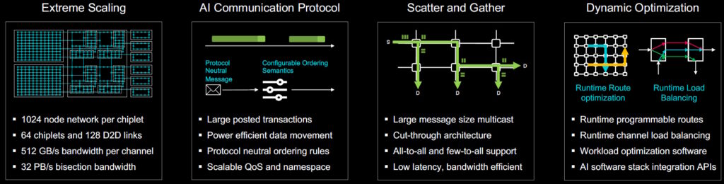
Scalable fabric for AI systems and data center applications
(Source: Baya Systems)
The combination of Weave IP and WeaverPro results in a unified design flow. The benefits of an intelligent data-driven unified fabric include a common transport mechanism that optimizes performance and area, extensive flexibility in topologies and scale, correct by construction (deadlock free, QoS, RAS), and workload-based local and global optimization.
Unified design flow (Source: Baya Systems)
In addition to static design-time configuration and optimization, WeaverPro’s APIs also support dynamic run-time analysis, customization, and optimization.
Advanced design and runtime optimizations (Source: Baya Systems)
Now, it’s easy to become carried away with all of this (you really should ask the guys and gals at Baya to give you a demo of it in action), but “the proof of the pudding is in the eating,” as they say, so what can we expect to see in the real world? Well, the results below reflect the effects of design time and runtime optimizations on a real-world design.
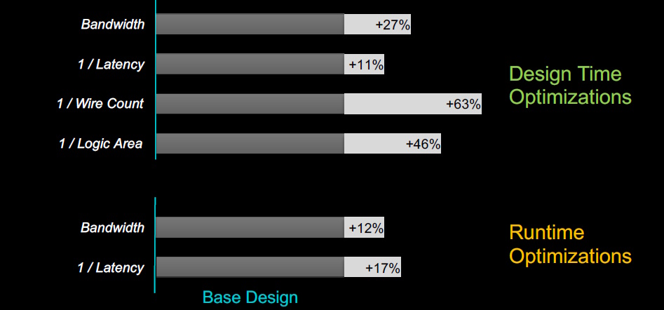
Results vs. baseline implemented using standard mesh (Source: Baya Systems)
The baseline for the design (the dark gray portions of the bars) was implemented using a standard mesh. The optimizations, which are all tool-driven, are reflected in the light gray portions of the bars (super users can use these results as a starting point to achieve further optimizations). There’s a lot to wrap our brains around here, but we can summarize Baya’s solution as follows:
- Software-driven architecture exploration helps optimize design to achieve performance guarantees based on built-simulator.
- An engine generates representative workloads from a traffic specification.
- Best-in-class, flexible network can achieve 3GHz in a 4-nanometer process technology.
- Algorithmic optimization supports reuse and minimizes silicon and power footprints without compromising performance.
- Industry’s first IP to offer multi-level cache coherency for single/multi-die systems, radically reducing costs of coherency across these large-scale systems.
- Customizable protocol and multicast capabilities for advanced AI and CPU acceleration that support petabyte-level throughput.
- Correct-by-construction design generation that radically reduces risk of failure.
- Weave IP supports standard protocols such as CHI, ACE5-Lite, AXI5, and is extendable to others including CXL.
- Physically aware flow with modularity and tiling support for ease of implementation.
I know you’ve heard me say this before, but when I designed my first ASIC circa 1980, I was on a team designing a CPU for a mainframe computer. We were working at the gate-level and capturing our designs using pencil and paper. We didn’t have any sort of design tools available to us. Logic optimization and minimization was performed by hand. Functional verification involved you walking the team through your design and defending your implementation decisions. Timing analysis involved us identifying the critical paths and calculating the wire and load delays. We didn’t even have an electronic calculator at our disposal (those were reserved for managers to calculate their lunch expenses).
We’ve come a long way since then. We couldn’t even have dreamed of offerings like Weave IP and WeaverPro—and we couldn’t have conceived of the designs these tools are capable of creating. How about you? Do you have any thoughts you’d care to share about any of this?


One thought on “Weaving State-of-the-Art Chiplet and SoC Fabrics”