


Before we dive headfirst into the fray with gusto and abandon (and aplomb, of course), let’s briefly remind ourselves as to the current state-of-play on the chiplet and multi-die systems front. Let’s start with the fact that artificial intelligence (AI) and machine learning (ML) are becoming pervasive and ubiquitous. Let’s also remind ourselves that we create our systems using a variety of processing elements, including CPUs, GPUs, NPUs, TPUs, and other hardware accelerators.
The way we design devices like ASICs, ASSPs, and SoCs today is that we purchase intellectual property (IP) blocks for commonly used functions from trusted third-party suppliers. These IPs might be processors, memory controllers, high-speed interfaces, etc. We also create our own “secret sauce” IPs that will differentiate our device from its competitors. All these IPs are known as “soft IPs” because they are represented at an abstraction level known as register transfer level (RTL), which is captured in the form of a hardware description language (HDL) like Verilog or VHDL. The IPs are subsequently integrated and synthesized into a gate- and register-level netlist that will be fabricated on the silicon chip. Everything in this paragraph is a gross simplification (apart from this sentence).
Some of the behemoth companies—like AMD, Intel (and newly spun-off Altera), and Nvidia—have the wherewithal to mount multiple silicon chips (a.k.a. chiplets) on a common silicon substrate. The result is known as a multi-die system. Other, smaller companies dream of having this ability.
At some time in the future, it will be possible for even small companies to purchase “hard IPs” in the form of chiplets, to create their own “secret sauce” chiplets (using the tools and techniques we currently use to design ASICs / ASSPs / SoCs), and have all these chiplets assembled on a common substrate and packaged in a single package. This day is getting closer. As per the 2025 Chiplet Summit, chiplet-centric tools, technologies, and ecosystems are currently sprouting like mushrooms.
Now let’s turn our attention to memories. Life used to be so much simpler when I was a lad. In the case of semiconductor memories (I’m excluding earlier technologies like mercury delay lines and magnetic core stores from these discussions), we had ROM and RAM, where the former was non-volatile (a.k.a. persistent), and the latter was volatile (a.k.a. transient).
When it came to RAM, we had two yummy flavors: Dynamic RAM (DRAM) and Static RAM (SRAM). Viewing things on a per-memory-cell basis, DRAM was cheaper, occupied less real estate, and consumed less power, but it was slower, while SRAM was faster, but it was more expensive, occupied more real estate, and consumed more power.
In the case of bulk storage, we had hard disk drives (HDDs). (Once again, I’m excluding earlier technologies like paper tapes and punch cards, otherwise we’ll never get started, let alone finished.)
We were as happy as clams, and then things started to get complicated…
To be honest, it’s getting to the stage where I’m finding it hard to draw a memory hierarchy diagram. The best I can do is the one shown below.
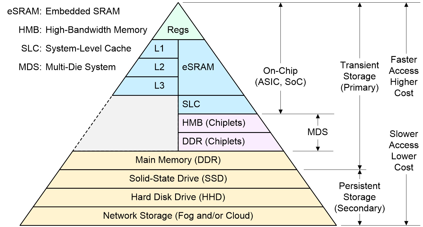
Memory hierarchy (Source: Max Maxfield)
At the pinnacle of the pyramid, we have registers that are embedded in the processors (CPUs, GPUs…). These can typically be accessed in a single clock cycle.
Next, we have the L1, L2, and L3 caches, also any embedded SRAM (eSRAM), also any system-level cache, all of which are typically implemented in SRAM.
The registers, caches, eSRAM, and SLC are all implemented on-chip. Historically, we then went off-chip to main memory in the form of DDR devices mounted on the printed circuit board (PCB). Commencing circa 2015, high-end ASICs, ASSPs, and SoCs started to include high-bandwidth memory (HBM)—a type of DRAM—in the form of die stacks connected to each other using through-silicon vias (TSVs) and connected to the main die via appropriate interfaces. Although we don’t typically think of HBMs as chiplets, that’s sort of what they are. And, more recently, we are starting to see DDR chiplets appearing on the scene (where DDR is yet another form of DRAM).
In addition to DRAM and SRAM, there are other types of memory, each with their own advantages and disadvantages. These include Flash Memory (NAND & NOR), MRAM (Magnetoresistive Random-Access Memory), ReRAM (Resistive Random-Access Memory), FRAM (Ferroelectric Random-Access Memory), and PCM (Phase-Change Memory).
MRAM is attractive for many reasons, including the fact that it’s non-volatile, it consumes lower power than DRAM, and it’s faster than DRAM. MRAM also consumes much less power than SRAM, but it’s significantly slower than SRAM… until now (cue drum roll).
The reason I’m currently squirming in my seat with excitement is that I was just chatting with Max Simmons, who is the CEO at Numem (think “new memories”). Max (no relation) was recently at the 2025 Chiplet Summit (Numem had a booth) rubbing shoulders with potential ecosystem partners.
Here’s the deal in a crunchy nutshell. The folks at Numem have created a memory technology called NuRAM. All the big semiconductor fabs (GlobalFoundries, TSMC, Samsung) have an MRAM process as part of their offerings. NuRam is based on these standard MRAM processes. The differentiators are Numem’s MRAM array architecture and its SmartMem subsystem, which results in MRAM IP with SRAM-like performance. Truthfully, I can’t say this better than the guys and gals at Numem; the following is from their website:
Based on standard MRAM production processes, Numem’s patented NuRAM memory enables best in class power, performance and reliability with 2.5x smaller area and 85x-2000x lower leakage power than traditional SRAM. Combined with the SmartMem SOC subsystem, it enables SRAM like performance and/or ease-of-use by enabling significant performance and endurance improvement, comprehensive adaptive memory management, along with optional and customizable SOC Compute in Memory.
The chaps and chapesses at Numem started by selling their MRAM IP and SmartMem IP as… well, as IPs, really. These IPs are used by the folks currently designing ASICs, ASSPs, and SoCs.
Now, the little rascals at Numem are gearing up to provide their NuRAM technology as packaged chips. Of particular interest (at least, to me) is that they are also gearing up to provide their NuRAM technology as chiplets. This explains why they had a booth at the 2025 Chiplet Summit—they are looking to work with ecosystem partners to provide reference designs for use by other players.
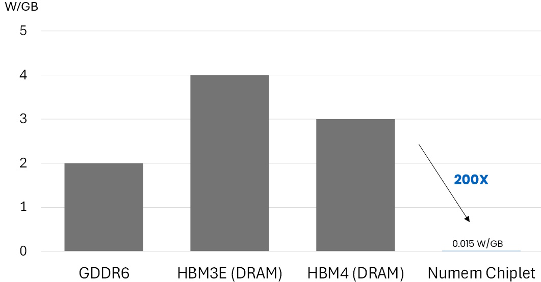
They already have a test chip back from the fab, the evaluation of which allowed Max (no relation) to provide me with the two charts shown below.

Bandwidth against AI memory module (Source: Numem)
Standby power against AI memory module (Source: Numem)
All of this allowed me to modify my memory hierarchy as shown below. As you can see, I’ve added the red bounding box showing the areas in which the folks at Numem can play. Also, I’ve added a red star to the “Transient Storage” because any functions implemented in NuRAM will be persistent.
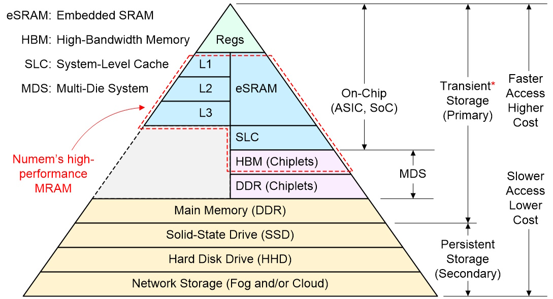
Potential places for high-performance MRAM to play in the memory hierarchy (Source: Max Maxfield)
Arrggggh. I just realized that, when the folks at Numem do start to offer their NuRAM technology as packaged chips, I’ll have to reflect this in an updated version of my diagram. Happily, that is something we can punt to another day.
So, what do you say? Do you have any thoughts you’d care to share on anything you’ve read here? As always, I await your comments in dread antici…


The diagram shows regs and L1, L2, L3 ESRam on chip.
It would be simpler and faster to simply implement a stack on chip and block memory for user data
since users must use malloc for storage space.
If the sram block memories have true dual port as Altera does, the number of cycles
to evaluate expressions decreases dramatically and performance increases dramatically.
Furthermore using C# instead of vanilla C allows conditional assignments.
For SOCs, caches and DDR interfaces may not be necessary because of the amount of block memory.
Hi Karl — thanks for your input — you make a good point — but I’m assuming an ASIC type of SoC here — not an SoC FPGA — in the latter case I agree that I might draw this diagram differently. Having said this, the caches associated with an Arm Processor cluster on an Altera SoC FPGA are implemented in eSRAM.
Thanx Max. Several things keep bothering me:
The rest of the world no loner uses C, but embedded is stuck with C and HDL. That is because of a stupid management decision “HDL can be simulated”. But the synthesis/tool chains only synthesize
what they want to/can synthesize which puts more limitations on designers.
I can find no justification for 3 levels of caches either. In fact I cannot find anything more than intuitive justification for caches. The whole cache concept was for matrix inversion applications.
(Yes, I was there when caches and DDR were conceived.) DDR was justified because of cache misses had to write modified cache lines before fetching new data to write into cache lines.
Although I cannot find it, a year or two ago you wrote an article about cache coherence does not work for all possible situations.
And I wondering if any designer will live long enough to complete and verify a design big enough to fill one of these humongous ASICs. BUT by putting all the things that you have in the diagram that is a different story.
I would like to read an explanation of why ARM(Advanced Reduced Instruction set Machine) has its roots on the same architecture as RISCV can be replaced by RISCV simply because it is open source.
I am so glad that Patterson got the Turing Award.
Hi Karl — there’s a column by the folks at Arteris (the folks who supply Netoork-on-Chip (NoC) IP) that does a nice job of justifying an L3 cache: https://www.eetimes.com/cache-memory-how-to-turbo-charge-your-socs-cpus/
And the thing that jumps right out is assuming a 95% hit ratio but no measurement.
And next is operator precedence which was a real nightmare until Professor Dykstra
invented the Shunting Yard Algorithm which uses a stack to handle precedence.
True dual port memory can push a result and pop the next two operands in one cycle.
And that is why this approach is so much faster than any RISC.
Well there is nothing about RISC or levels of cache that are significant.
Furthermore C users use malloc to get storage space for operands which ends up as a stack.
Stack based evaluation uses Push/Pop operations instead of load/store which is important because a stack can be implemented as a true dual port Ram using embedded memory blocks.
Intermediate results are simply pushed onto the stack. Each operator evaluation consumes one stack location so at the end the only thing on the stack is the expression result.
And the user is not required to code loads and stores because the compiler API manages the
reading and writing of operands which are also kept in on chip Rams.
There are no arithmetic or logical instructions since everything is done as expression evaluations.
So all of that load, store, add, subtract, compare, branch stuff does not have to be coded in C.
5