


Anyone who’s anyone has at least one AI angle working for them. Unwilling to settle for just one angle, Mentor Graphics discussed two angles at this summer’s DAC. As an EDA company, they have two specific opportunities to find value with AI. One is to improve the design tools they provide; the other is to create design tools specifically for AI designs. Very different things (although the latter might be used internally to benefit the former). We’re covering the first today; we’ll look at the second one soon.
So, for this story, AI won’t be an end in and of itself; it will be the means to an end. AI has been used in production floors to help increase yields and reduce equipment excursions, but that relies on manufacturing data in the foundry. Today we’re moving upstream from the production environment to the design world. We’ll specifically look at how Mentor is leveraging AI for both optical proximity correction (OPC) and design-for-manufacturing (DfM) within foundries.
AI in OPC
Let’s start with OPC. For anyone new to the notion, we’re at silicon feature dimensions far too small to be printed by 193-nm light. And so we play tricks to get it to work. The problem is that features are so close to each other that they interfere with the fidelity of each other’s shapes. So the shapes are modified – or “assist features” are added – to fool the light into doing what we actually want. This is OPC.
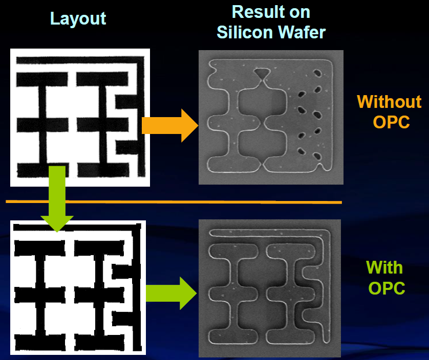
(Image courtesy Mentor Graphics, a Siemens business)
OPC is classically done using deterministic models that allow a tool to create the modified pattern. But Mentor says that there are four challenges with OPC:
- Accuracy
- Turn-around time (TAT)
- Process window enhancement
- Productivity
They’ve targeted the first two for help using AI. (The window-enhancement notion is something we’ll talk about more in the future.) The issue is that, in order to achieve the needed accuracy, the number of cores required to complete OPC within 24 hours is increasing dramatically. They see AI as a way to bring this down.
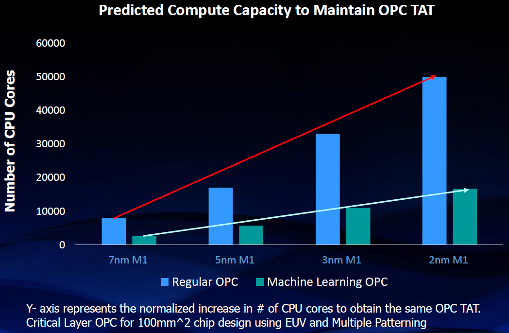
(Image courtesy Mentor Graphics, a Siemens business)
OPC is an iterative process, requiring in the range of 10-15 iterations to converge. Mentor’s approach is to use machine learning to handle, in one fell swoop, the first 10 or so of those iterations. This may not result in a good-to-go mask, but it gets a whole lot closer. Traditional iterations can then be used – just a few times – to get the final result.
As you can see from Mentor’s graph above, the number of cores required for a 24-hour turn drops by two thirds. Another way to say this is that the TAT with AI is one-third that of the traditional approach – while improving accuracy.
The data used to train the models is based on initial foundry design measurements. In order to determine the full process window, a design-of-experiments (DoE) is done to broaden the data set. New designs can then leverage this model for OPC.
Models Evolve
Of course, one of the interesting characteristics of AI is that learning never stops. The more data you get, the better the models become. So, in theory, one could keep taking manufacturing data beyond the initial lots and continue working it into the AI model so that it improves over time. But there’s a catch here.
Let’s say you’ve taped out a design and you find the need for a change. You activate the engineering-change order (ECO) process and make the tweak. You’re now going to generate a new mask, which requires OPC. But, in this hypothetical case, let’s say that the OPC AI model being used for this tweaked design has evolved beyond the one used on the original mask set. So now, when you run OPC, you may change not only the parts of the circuit affected by the ECO, but, in fact, the entire mask.
Is that OK? Do you trust that AI-model evolution only improves things? Or could you end up with something that used to work no longer working? We’d like to think that, even though tons of unexpected stuff changed, it changed for the better. But do you now need to run some tests to make sure that nothing broke? This violates that cardinal rule, “If it ain’t broke, don’t fix it!” So how do you deal with this?
I asked Mentor, and it sounds like there isn’t a solid policy on this yet. They pointed out that, when new hot spots are identified, the first priority is to make selective manufacturing tweaks to bring yield back up, if possible. But that change can then be worked into the AI model, allowing it to highlight even more problem areas of the die. So the “continuous learning” model is a real possibility.
I suggested one possible way of handling this, which they agreed was an option. That way is version locking. This is a concept already in place for design tools, since new versions may change algorithms, and changing versions in the middle of a design may undo all the convergence work already done. So you lock the tool version for the life of a design, moving to the new version on the next design.
This could also be done with OPC (or any other) AI models: lock the version of the model to the design so that any future work done on that design will use the same AI models. That said, there’s probably one exception: if this is the design that uncovered that new hot spot – the reason the model got changed in the first place. Yes, tweaking manufacturing is ideal, but, if it’s not enough by itself, you may need to change the mask to eliminate that hot spot. Using the new model in this case would make sense.
All of that said, it feels to me that we’re wading into unsettled territory here, so there may be a number of policies that dictate what to do in this case. File under “T” for “TBD.”
AI for Finding Hot Spots
I first must confess some confusion about which product this applied to. It looks a lot like DRC, but it turns out that it’s for library validation. In other words, this isn’t a tool that you as a designer would use; it’s a tool that the foundry uses when putting together their circuit library. It’s for finding yield-limiting hot spots by pattern, and those runs typically need to be able to complete overnight. Full simulation takes too long, so vulnerable patterns are sampled and checked during these runs. Those vulnerable patterns are found in a pattern library (separate from the circuit library being validated).
What’s new is that, instead of using the library for the check-out, they use it to train an AI model and then use the AI model to check out the circuit libraries. This brings a couple of benefits. First off, if they use only the models in the library for checkout, as has been done for years, then you’ll find only those specific patterns in the design. But, using AI, you may find other patterns that are similar but aren’t in the library. So you get better quality and, hopefully, higher yields.
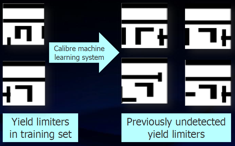
(Image courtesy Mentor Graphics, a Siemens business)
The other benefit is that now the checkout runs 10 times faster than it does using the traditional model. And this claim bears some explanation. Doing full library simulation takes a really long time, which is why check-out is often limited to specific known hot-spots. When sampling hot-spots, coverage isn’t exhaustive. So when we say the AI-assisted version is 10 times faster, which thing are we comparing to? I checked with Mentor, and they confirmed first that the AI version is exhaustive. And the 10x comparison is as compared to full simulation – that is, we’re comparing exhaustive (old) to exhaustive (new).
More info:
Sourcing credit:
Dr. Steffen Schulze, VP Product Management, Calibre Semiconductor Solutions, Design to Silicon Division, Mentor Graphics


What do you think of Mentor’s use of AI for litho-friendly design?