There is an interesting side effect of Moore’s Law’s relentless march, where some technologies atrophy even though they are still extremely relevant and applicable in the mainstream. Take, for example, the case of the 100K LUT FPGA. Not that many years ago, a 100K LUT FPGA was solidly in the high-end, and numerous applications took advantage of the generous helping of flexibility and hardware programmability that such a device brought to the table. At that time, the big FPGA vendors charged a premium for these devices, and customers lapped them up with glee.
After a generation or two of Moore’s Law, however, these devices fell into the “mid-range” category. Xilinx and Altera built cost-reduced devices in that density range that had modest but usable IO, on-chip memory, and hard IP resources. These devices served the market well for a decade or so.
But, as time continued, the interfaces, memory, and IO of these chips started to get long in the tooth. Even if the programmable logic was enough for your application, the other aspects of the chip might not easily support the current standards your design required. As a result, many of these chips have slowly faded from relevance, leaving a hole in the market in that very useful density range.
Nature may abhor a vacuum, but savvy semiconductor marketers see opportunity where gaps emerge.
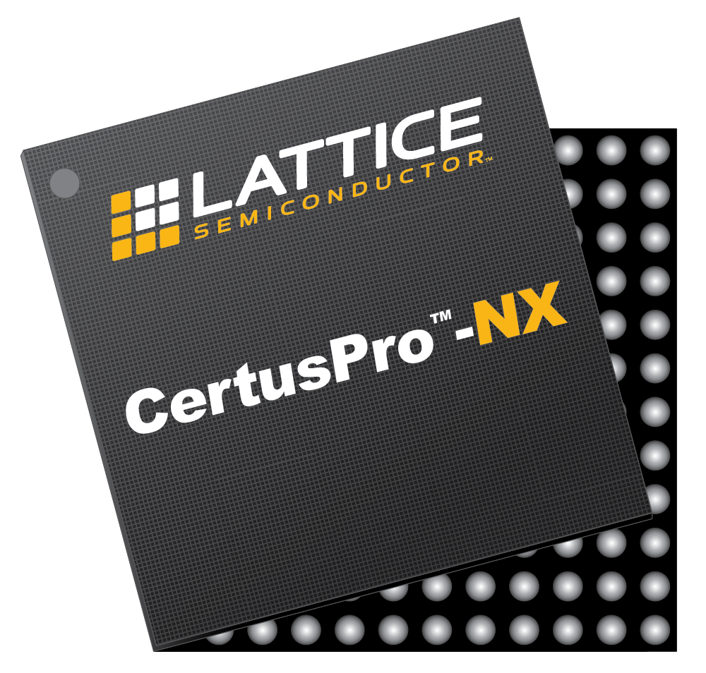
Lattice has been capitalizing on the opportunities in mid- and low-range FPGAs for years now, and their latest announcement – a new general-purpose FPGA family dubbed CertusPro-NX. The “Pro” in the name, of course, tells us they are serious about it this time. Perhaps those old families were just for amateurs? Regardless, CertusPro-NX is a worthy modern-day FPGA with compelling capabilities that clearly set it apart from its aging rivals. Move over, grandpa, there’s a new mid-range kid in town.
Hitting the high points, CertusPro-NX brings lower power programmable fabric (thanks to FDSOI technology and a power-friendly architecture), modern IO capabilities – including 10Gbps SerDes, modernized edge processing capabilities (using new DSP blocks, generous on-chip memory resources, and DDR3/LPDDR4 interfaces), and smaller form factor owing to 0.5mm pitch packages down to 9x9mm. Together, this brings all the goodies we’d want in an FPGA with modest requirements for programmable fabric.
Focusing in on the power aspect, Lattice claims that CertusPro-NX can achieve “up to 4x lower power” (or, as we’d say, 80% less power) than comparable Intel Cyclone or Xilinx Artix/Kintex devices. In edge applications with limited power budgets, this is of course a big deal. Lattice has also focused on design decisions that should help minimize total system power beyond just the savings in the device itself.
The SerDes transceivers in CertusPro-NX are capable of achieving 10.3 Gbps, whereas most competing devices top out at just over 6 Gbps. The difference, then, is support for 10G Ethernet as well as a number of other useful current standards. The combination of these higher data rates with smaller form factor should slide CertusPro-NX into a number of sockets where other devices simply can’t compete.
Many of the current applications for FPGAs land in the realm of compute acceleration. Lattice has targeted edge acceleration with the new family by beefing up the memory and DSP resources on the chip, optimizing the architecture for AI inference in particular, and supporting LDDR4 memory in order to tackle edge inference situations other mid-range FPGAs cannot handle. Lattice says CertusPro-NX has up to 65% more on-chip memory than comparable-density Artix and Cyclone devices.
The proliferation of these devices at the edge places new demands on reliability as well. Lattice says that the FDSOI technology, along with other architectural features of the chips, gives CertusPro-NX better thermal performance, extended temperature ranges, and a “100x lower” (Here we go with that again. How about 99% lower?) soft-error rate (1B-hour failure-in-time “FIT” rate). This makes the devices a great choice for industrial and other high-reliability applications with demanding environmental requirements.
And, with form factors continuing to shrink, design teams will be happy with the available 9x9mm packages with 0.5mm pitch. This puts CertusPro-NX in a class by itself if board real-estate is at a premium. Competing devices range from 121mm2 to over 500mm2, so Lattice brings in significant space savings with a more capable chip.
We have also written about Lattice’s solutions-oriented strategy these past few years, which is based around “solution stacks” that include IP, software, firmware, reference designs, development boards, and pretty much everything else you’d need for a near-turnkey solution in key application domains. Lattice says CertusPro-NX will be supported by their “SensAI” low-power edge AI stack, their “mVision” low-power vision stack, and their new “Automate” factory automation acceleration stack. These stacks should make it easy for teams in these application areas to take advantage of CertusPro-NX without having to hire FPGA experts and spend months on custom designs.
This is obviously a big announcement for Lattice, and it falls directly in line with the strategy the company has been pursuing for the last several years. It is interesting to see Lattice doing direct, head-to-head comparisons with competitive devices from Xilinx and Intel, and it shows a confidence in their technology and their strategy that comes from numerous recent successes in the markets they have carved out for themselves.
It will be interesting to watch Lattice’s performance in these markets, as well as how the markets themselves grow. Most forecasts call for a huge increase in applications that demand edge acceleration capabilities, and Lattice has staked a position that should give them a leg up, even if their larger competitors re-focus their attention on the mid-range market. And, given that AMD is acquiring Xilinx, and Intel has been re-molding their FPGA offerings primarily to support their data center business, it’s unlikely that Lattice will see any significant competition any time soon in this arena.


