Lattice Semiconductor has a knack for finding and exploiting holes in the programmable logic market. Years ago, they gave up chest beating their way into a distant third place in the FPGA market and decided instead to concentrate on the areas that the two dominant players (Xilinx and Intel/Altera) were ignoring. In a broad sense, that meant low-end FPGAs – devices with small form factors, small price tags, and very low power consumption. In support of that strategy, they launched lines of well-focused low- and mid-range FPGAs and acquired SiliconBlue – a startup that was making extra-tiny FPGAs for high-volume applications such as smartphones and mobile devices. In an era when the other FPGA companies were touting “world’s largest” and “industry’s fastest” superlatives, Lattice differentiated themselves with “World’s Smallest FPGAs” as their marketing catch-phrase.
This strategy has, by-and-large, worked out well for Lattice, and, after surviving a wake of reorganizations, headquarters relocation, and a failed merger attempt, the company seems to have emerged with a solid strategy, a strong product portfolio, and a loyal customer base. In fact, because of the high-volume markets Lattice’s devices serve, it is very likely that they have shipped more FPGAs than any other company on the planet.
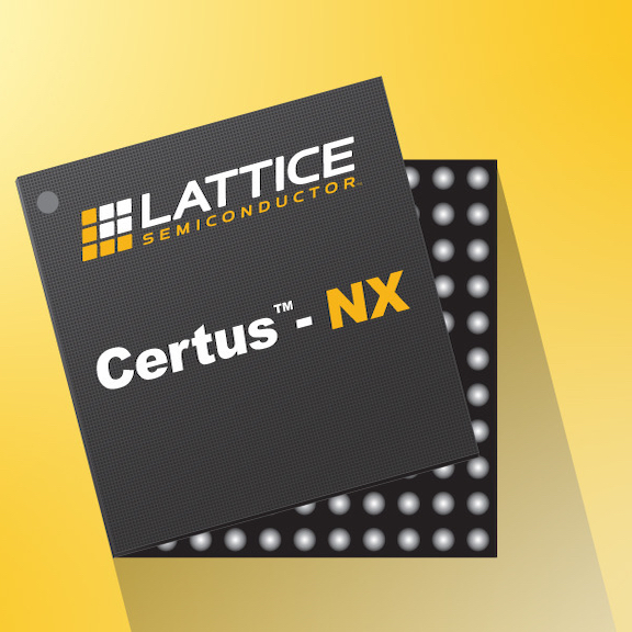
Now, the company is launching the newest of their low-end wonders – Certus-NX, a well-conceived new family of general purpose low-end FPGAs fabricated on low-power 28nm FD-SOI technology, which brings very good performance/power characteristics (Lattice claims 4x lower power vs similar FPGAs), high reliability, high immunity to SEU events (Lattice claims 100x lower soft-error rate), and low cost. Lattice has clearly designed Certus-NX as an IO-heavy family, with a very high ratio of IO capability to core logic (Lattice says 2x more IO per mm2 vs similar FPGAs). This is a smart move on Lattice’s part, as it fits the devices nicely to a bevy of current and emerging applications – particularly in edge applications that require bridging or processing. Lattice says Certus-NX is targeting applications “from data processing in automated industrial equipment to system management in communications infrastructure.”
Certus-NX has two family members, the LFD2NX-17 and LFD2NX-40. These devices had 17K and 39K logic cells respectively, 432K and 1,512K bits of EBR embedded memory, 2,560K and 1,024K of large memory, 24 and 56 18×18 multipliers, 2 ADC blocks (12-bit, 1 MSPS), 2 and 3 GPLL, 2 SGMII CDR at up to 1.25 Gbps – to support 2 channels SGMII using HP I/O (for Gigabit Ethernet), and the larger device adds a 5 Gbps PCIe Gen2 hard IP block. Depending on package selection, the devices have up to 192 total programmable IO. Packages are as small as 6x6mm, with ball-pitch options of 0.5mm and 0.8mm.
Lattice says Certus-NX is “Instant-on” (we might say “almost-instant-on,” but we are nit picking). IO configures in 3ms and the full device in as little as 8ms. IO can be configured independent of the core logic, which allows more robust system startup and in-system reconfiguration options with what Lattice calls the TransFR field upgrade feature. Because the FD-SOI process allows programmable back-bias, the devices can be configured as “low power” or “high-performance” depending on your particular application needs. Bitstream security is provided by ECDSA bitstream authentication and AES-256 encryption.
Certus-NX is supported by Lattice’s Radiant design software, with synthesis library support available for popular logic synthesis tools. Radiant takes your synthesis tool output, combines that with constraints generated by Radiant’s floorplanning tools, and uses that to drive place and route. Radiant then extracts timing from the routing and back-annotates it into your design for timing verification. Lattice also provides a rich library of pre-engineered IP blocks that are compatible with Certus-NX, and lots of third-party synthesizable IP can be used as well.
Lattice expects Certus-NX to be used in applications such as PCIe-to-SGMII bridging, PCIe control plane bridging, co-processing by offloading compute and DSP tasks from applications processors, motor control, and more. For co-processing, the 18×18 multipliers will come in handy, and the DDR3 and LPDDR2 interfaces should give robust options for data buffering. The LUT fabric, while not enormous, is enough to potentially do lower-complexity neural net inference tasks as well.
These devices sit at a largely uncontested spot in the FPGA market. Xilinx and Intel give little-to-no attention to their smaller-sized devices (which haven’t been updated in years). Microchip/Microsemi is going after the lower densities, but they are aiming at higher-density applications than Lattice and are more focused on high-reliability applications. The closest comparisons of competing FPGAs would be Intel’s Cyclone V and Xilinx’s Artix-7 (neither of which have been updated in years). Because of the FD-SOI technology and Lattice’s architecture, Certus-NX is likely to have dramatically lower power consumption, faster reconfiguration, smaller footprint, and more robust IO, while sporting slightly lower density.
Lattice says samples of Certus-NX are already shipping (Lattice has always been more conservative than competitors, choosing not to “announce early” with new families.) Design tools are available immediately.


