Flash memory technologists had a problem. Their customers needed more memory, and so they were trying to make the memory cells smaller so they could fit more onto a chip. But the demand was growing faster than the technology was shrinking, so they needed to get to higher densities more quickly.
The basic flash memory cell had traditionally stored one of two values: a 1 or a 0. They read the memory by detecting the amount of charge in the cell: a lot meant 0; a little meant 1. But they had enough slop in there – meaning that they could read more accurately than they were giving themselves credit for – to add some levels between 1 and 0. First they did a cell that had four levels; then they did a cell that had eight detectable levels. The original bit cells each stored 1 bit; the next wave stored 2 bits each; and the third version stored 3 bits per cell.
With all that work, on a given technology node, they had now tripled the amount of memory available in a roughly equivalent footprint.
Following Memory’s Footsteps
While it might not be accurate to say that communications technologists specifically took their cues from memory, they nonetheless have done more or less the same thing as the flash folks – or at least the first step (so far). Instead of a physical layer that provides 1 bit of information per cycle (or some other time slot), they’ve doubled the data throughput without changing the operating clock frequency.
This format is known as PAM-4*. “PAM” stands for pulse-amplitude modulation, and the “4” means four levels. We’ll go through a little review for those of us (like me) that aren’t completely steeped in this stuff.
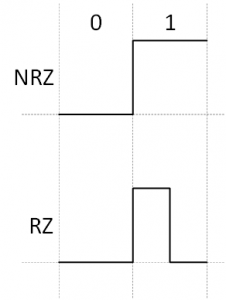
Traditional voltage waveforms for high-speed signaling have traditionally been NRZ – non-return-to-zero – in format. A high voltage indicates a 1; a low voltage indicates a 0. The name contrasts this format with RZ, or return-to-zero, which is more pulse-like. A 1 might be indicated by the signal going high, but then it returns to 0 instead of remaining high for the duration of the symbol. A 0 bit would be indicated by no pulse.

Instead of stopping at two levels, PAM-4 subdivides the vertical axis to provide four distinct levels:

This doubles the amount of data you can send in the same timeframe. For example, to send a “3” would require two symbols using NRZ: 11. PAM-4 does the same thing with one symbol.

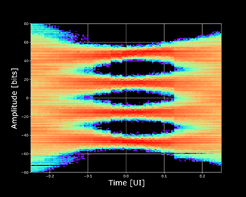
Of course, it’s easy to do a line drawing showing how this works. Creating real, live transceivers that can do this isn’t so easy. In fact, one theory is that this originated as something that would specifically be hard – even impossible – for many companies to accomplish, providing a competitive advantage to those that could. After all, we’re still talking about eye diagrams here – it’s just that they’re stacked. If you thought a binary eye diagram was hard to do, then – trigger warning – you might not want to look at the following eye diagram. (Except that this warning is probably too late.)

(Image courtesy eSilicon)
We’ve seen PAM-4 supported in the new Intel Agilex FPGA family, and eSilicon now has a PAM-4 transceiver implemented on 7-nm silicon. With this, they achieve 112 Gbps – up from 56 Gbps using NRZ. In fact, this is exactly double what can be done with NRZ, which is not by accident. eSilicon’s transceiver can still do NRZ if needed, giving 56 Gbps, which is useful as the transition from 56 to 112 progresses.
Ethernet is a particular target for this transceiver, although the circuit is protocol-agnostic. For instance, FibreChannel could also benefit.
It’s not simply a matter of doubling everything up, however. These are obviously more delicate signals to detect, and inter-symbol interference can cause problems. PAM-4 uses a decision-feedback equalizer (DFE) to help with that, but that can cause correlation errors. For that reason, PAM-4 at 112 Gbps needs forward error correction (FEC), which has an impact on latency.
It’s possible that, as technology improves, the bit-error rate (BER) will drop, making FEC unnecessary. For example, today, eSilicon says that you could run 30-Gbps PAM-4 signals without FEC. But we’re not there yet at the top speeds.
Playing the Long Game
While this double-speed capability is exciting, it’s just now entering the market at the silicon level. Heck, as eSilicon tells it, infrastructure for 56 Gbps is still coming on. So it will be a couple of years before we see the fruits of the PAM-4 efforts and 112 Gbps.
Even so, there are already musings on what we could do to get to 224 Gbps. I know, you give and you give, and you do and you do, and it’s never enough.
- One obvious way to get to 224 would, of course, be to move to a process node that allowed you to double the clock frequency and then use PAM-4.
- Another way would be to create a full-duplex channel. While either direction would be sending data at 112 Gbps, there would be 224 Gbps on the line – 112 forwards and 112 backwards. You could do this today with half-duplex or with two independent channels – one to and one from. It’s the combining onto a single channel that gets complicated.
- And then there’s the other obvious way (in concept) to double speed: go from PAM-4 to PAM-8. Yes, there is talk about this, but nobody’s working on an actual spec yet, according to eSilicon. So it’s probably 5 years or more over the horizon.

The drawing illustrates conceptually what’s happening here, which involves two things. First, the obvious one: we move from four levels to 8. Less obvious is a possible increase in overall swing. The drawing shows something less than double the total swing. I want to be clear that that was strictly for the convenience of the artist (me – OK, so I’m not really an artist; you got me!). Where that swing would end up is, of course, part of the standard-setting negotiation.
The wider the voltage range, the easier it becomes to discriminate the intermediate levels. But, if you had a signal going from 0 to 7, then it would have a higher swing to traverse, which either takes longer or is harder to design (or both).
Nonetheless, just as flash memory wasn’t satisfied with doing only four levels per cell, so PAM is also likely to get itchy to repeat the original success and go to eight levels. My guess is it won’t be trivial. But, presumably, the lessons learned from the first non-binary signaling can inform the next round.
*PAM-4 is also written PAM4. Wikipedia includes the hyphen, so I have as well.
More info:
Sourcing credit:
Mike Gianfagna, VP of Marketing, eSilicon
Tim Horel, Director of Field Applications, eSilicon


What do you think of PAM-4 as a new signaling format?