It was the best of DRAM access times, it was the worst of DRAM access times…
Do hybrid devices combine the best of two technologies, or the worst? Is a Toyota Prius a great leap forward, or just a small gas-powered car lugging around a heavy battery in its trunk? Peanut butter and chocolate, or floor wax and dessert topping?
How about DRAM volatility combined with flash memory’s block-erase cycles – a good combo or a terrible idea? Let’s complicate the decision. What if it were faster than DRAM, used less power, and had four times the density? What if it cost less per bit than today’s DRAM? Would you use it then? Have I run out of question marks?
We may eventually be able to answer some of those questions, courtesy of a small Singaporean company called Unisantis. The company presented a paper last month that describes its research into “dynamic flash memory (DFM),” a hybrid device that combines aspects of – you guessed it – dynamic RAM and flash memory. It’s purported to be the best of both worlds and a game-changer in memory technology.
To be clear, Unisantis has not fabricated any of these devices yet. It’s only simulated them. “By utilizing TCAD simulation, Unisantis has proven DFM has a substantial potential to increase density 4× compared to DRAM,” says the company. It certainly looks promising, but early simulations often do. Having said that, Unisantis is headed up by Fujio Masuoka, the man credited with inventing both NAND and NOR flash memories during his time at Toshiba, so there’s no shortage of talent or experience.
The key component, as it were, of the Unisantis DFM is a capacitor-free memory cell. Normal DRAMs use a transistor paired with a capacitor to hold a tiny charge that represents the 1 bit or 0 bit in that memory cell. Capacitors leak, so they have to be recharged at regular intervals, a process hardware designers know as a refresh cycle. Reading the bit also drains the capacitor, which DRAM chip designers patch up with a sense amplifier and a hidden internal re-writing cycle. In short, DRAMs are a nuisance. But they’re cheap, and cost overrides everything else in the high-volume memory business.
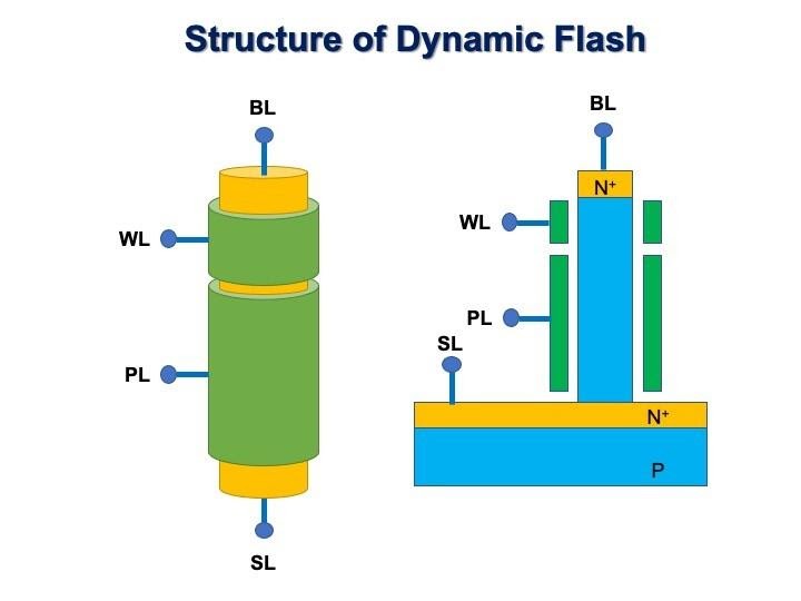
Unisantis does away with the capacitor and instead uses a second transistor to hold the memory bit. Normally, that would be a terrible idea. Doubling the transistor count merely doubles the size of each DRAM cell, which is exactly what you don’t want. But Unisantis puts its second transistor underneath the first one. They’re stacked vertically, like most NAND flash designs. (See where this is going…?)
Unisantis calls this its Surrounding Gate Transistor (SGT) because the lower storage transistor is cylindrical. A central silicon “pillar” forms the source and drain, which is wrapped in a bagel dog of a gate, as shown below.

Figure 1: Unisantis Surround Gate Transistor. BL = bit line, WL = word line, PL = plate line, SL = source line. (Source: Unisantis)
The device is still volatile, because the memory transistor still leaks – just not as badly as a capacitor. That means dynamic flash memories still have to be refreshed, but less frequently than with conventional DRAMs. This ought to save power, and should also slightly increase memory bandwidth, since you won’t have to pause read/write accesses so often to avoid refresh cycles.
On the other hand, dynamic flash memories are not bit-erasable. A side effect of the SGT design is that you can flip the storage transistor from a 0 to a 1, but not vice versa. To change from a 1 to a 0, you must first erase the memory cell, like a flash device. Unisantis also says that such erasures happen in blocks – also like a NAND flash. This makes writing to a DFM less like writing to DRAM and more like the read/erase/write cycle for a flash chip. The presentation suggests that such erase cycles will take 20–30 ns. No word on whether wear-leveling is required.
On the plus side, Unisantis says its patented SGM cell doesn’t need any exotic materials or fab processes. “DFM does not involve adding additional materials on top of a standard CMOS process…”
The company is quick to throw shade at ZRAM, MRAM, ReRAM, FRAM, PCM, and other memory types as mere “emerging memory technologies,” which seems a bit pugnacious, given the early state of its own research. The company was formed in either 2004 or 2008 (its literature contradicts itself) and has fabricated samples of interesting SRAM technology, but DFM is its first foray into DRAM alternatives.
Unisantis has yet to fabricate its first prototype sample of an SGT, much less a full DFM, but it’s obviously proud of its simulations, saying it has completed “extensive 3D process simulation for full integration of nMOS/pMOS devices and local interconnect; simulation includes lithography, deposition, and etch process window analysis, plus extraction of electrical model parasitics. Unisantis is continuing to work with its partners to achieve full SGT process fabrication and qualification, plus the development of compact device models for circuit design.”
If all goes well, Unisantis believes its SGT cell design can be up to four times smaller than today’s DRAM cells. This would obviously be a huge win for the memory industry, if true. The usage model is a bit wonky because it requires both refresh cycles and block-erase cycles, but those aren’t insurmountable hurdles. The key is cost. If DFM achieves the density improvements it claims, it should be cheaper to fabricate than conventional DRAMs, at least on a per-bit basis.
“In the mainstream memory market cost is everything, and specifications come second,” says Jim Handy, General Director of market researcher Objective Analysis. “If DFM can be manufactured using a standard CMOS process at smaller nodes than DRAM, without using any new materials, it could achieve a sufficiently low cost structure to compete effectively against DRAM despite the requirement for a block erase.”
DRAM makers scramble for even single-digit reductions in cell area; a 4× improvement would be spectacular. And users would likely be willing to overlook DFM’s hybrid nature if it means cheaper memory. Technology is hard, but economics is unforgiving.


