EMI is the ghost in our machines, the phantom of our electronic operas. We create our systems with a specific purpose, and our engineering efforts aim to hone and optimize toward that goal. At the same time, lurking in the copper traces and wayward return paths are silent specters seeking to derail our plans. They haunt our designs undetected, biding their time until the final day of reckoning, when they make their presence known, trashing our schedules and wreaking havoc on our best laid plans.
They say there are two types of engineers – those who design antennas on purpose, and those who design them by accident. Friends, ALL of us fall into that second category. And, we seldom realize it until too late, when some prototype begins EMI testing and we discover that the nagging feeling of unspecified dread that has kept us awake at night was real, and we have a problem that will require some serious re-design. Wouldn’t it be cool if we could simulate our entire system and catch those problems earlier? Or, in an ideal world, have tools that would guide our design so we never created the problems in the first place?
Cadence Design Systems recently announced Cadence Clarity 3D Transient Solver, a “system-level simulation solution that solves electromagnetic interference (EMI) system design issues up to 10X faster than legacy 3D field solvers and offers unbounded capacity.” Just to break that quote down a bit, the parts that should be in bold type are “system-level” and “unbounded capacity.” The field solvers required to do EMI simulation are enormously computationally complex, and doing such a simulation for a real-world “whole system” has traditionally been considered impossible, or at least grossly impractical.
Cadence has created what they call a “massively parallel matrix solver” that tackles this task with a combination of algorithmic cleverness and brute force parallel computing. And, while the parallel computing portion of that may seem obvious, it is absolutely not the norm for EDA tools. Most of the EDA algorithms in use – even today – were created and optimized in the era of single-core computing, and they do not usually adapt well to parallel computing. They have deeply embedded data dependencies that cause parallel processors to spend a lot of time sitting around waiting for each other to finish something. (It’s a lot like a modern office environment, really.)
In order to get the real benefits of parallel computing, EDA companies have had to go back to ground zero and develop entirely new algorithms that approach problems differently and allow massive scaling, and that’s what Cadence has done with Clarity. But this is not an easy or inexpensive task in the world of EDA, which is built on hundreds of millions of lines of code and decades of accumulated knowledge centered around ancient algorithms.
Of course, creating new, scalable algorithms is nice and all, but that still means you need an absurd amount of hardware in order to take advantage of them. That’s where Cadence’s cloud architecture comes into play. By making tools cloud-friendly, Cadence has provided the option for unlimited scaling. When you need really large amounts of hardware to solve a problem, it’s as close as the cloud (well, and your company’s budget office).
But, back to the problem of EMI for a moment. EMI compliance is typically one of the last steps in a design, and it often really waits until there is prototype hardware. There are several reasons for this. First, the kind of design errors that lead to EMI leaks are often done at the end of the development process, when prototype boards are replaced with production units and those few traces or connectors that were “optimized” at the last minute begin broadcasting like Pirate Radio. “Oops, uh, boss, we need to make a few last minute tweaks to the design here…”
And, EMI analysis does not subdivide well. In order to know what is happening with the system, we really do need to simulate the entire system. Problems with EMI don’t happen in isolation. We get interactions between the chips and traces on our boards, the connectors and cables that hook them together, and our mechanical enclosures. System-level understanding of the problem is essential. And, speaking of things needing to work together, Cadence says the Clarity 3D Transient Solver also offers “unparalleled integration with Cadence Virtuoso Layout, Allegro PCB Designer and SiP Layout.”
By giving us the practical ability to simulate and catch EMI problems earlier in the design cycle, Clarity has the potential to significantly shorten project schedules. Cadence customer Ultimate Technologies says they estimate they will be able to shave up to three months off their project schedules as a result of the new Clarity technology.
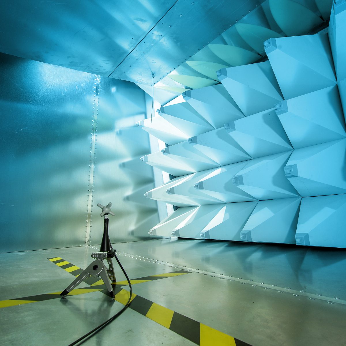
And, moreover, Clarity promises to make the project endgame more deterministic. With this capability, we can reduce or eliminate our reliance on anechoic chambers, expensive test equipment, and prototype hardware to suss out stray signals. And, best of all, we can all start getting a good night’s sleep before our system goes in for final EMI compliance testing.


