There are obvious attractions to “computing at the speed of light” with photonics-based technology—not just the extremely high speed, although that’s important, of course, but also the extremely low power as compared to transistor-logic-based computational implementations.
I’ve been exposed to a few companies offering various flavors of optical computing solutions over the course of the past couple of years. Until now, however, these have all predominantly involved injecting multiple beams of light at different frequencies and phases into lengths of optical fiber and using interference to perform complex calculations that would require humongous numbers of transistors had they been performed in silicon.
Well, I’ve just been exposed to something new and exciting on the optical computing front. I was chatting with Dr. Michael Förtsch, who is the CEO at a German startup company called Q.ANT. Of course, when I say “startup,” we need to bear in mind that Q.ANT was formed in 2018, which is six years ago at the time of this writing. I don’t know about you, but six years in the past seems like a lifetime away to me technology-wise.
To provide a little backstory, Michael started off on the computing site of things, but he got bored, so he moved into studying math and physics, and ended up with a PhD from the Max Planck Society. Michael then spent a couple of years working in the US at the National Institute of Standards and Technology (NIST), plus some other stuff, before he decided to move back into industry to form Q.ANT.
Before we proceed, it’s well worth noting that the sheer quantity of computation we (humans) wish to perform is now doubling every three months or so. That’s terrifying on multiple levels.
One issue here is the amount of energy we are consuming to perform our computations. Currently, most of these computations are performed using silicon chips based on CMOS technology. Smaller transistors consume less power than bigger ones. We are moving to smaller and smaller process nodes in which the dimensions of transistors are measured in nanometers, so that’s good—right?
Well, the problem is that the exponentially increasing amount of computation we wish to perform means we need to put tens of billions of these transistors on a single chip. Tens of billions of transistors consume a lot of energy, which is compounded when we have multiple such chips in a server, multiple servers in a rack, and tens of thousands of racks in a data center.
The bottom line is that our current computational solutions are (a) nowhere near as fast as we would like them to be and (b) consuming too much power. For example, Michael noted that he was at a supercomputer conference and exhibition recently. He says that every rack needed to be water-cooled. He also noted that new hyperscalar data centers are going to start requiring their own dedicated power stations—possibly in the form of small modular reactors (SMRs)—in the not-so-distant future.
Q.ANT in an interesting company. It boasts 100+ experts spanning 21 nationalities with ~890 years of industry experience and an average age of ~36 years. The company’s mission is to develop photonic computing solutions to address two of the major challenges in today’s artificial intelligence (AI) era:
- Managing vast data volumes (including complex mathematical operations) required for AI inference and other data-intensive applications.
- Significantly reducing the extraordinary amount of power and energy consumed in today’s AI-driven data centers worldwide.
Now, at this point we could dive deep into Q.ANT’s technology, but I fear a deep dive might obscure the bigger story, so let’s keep things at a relatively high level. Let’s start with the following image of a photonics-based Native Processing Unit (NPU) built on the company’s Light Empowered Native Arithmetics (LENA) architecture.

Q.ANT’s photonic chip at the heart of LENA (Source: Q.ANT)
The first differentiator to anything else out there is that this photonic chip is fabricated using Thin-Film Lithium Niobate (TFLN). Observe the low-loss waveguides on the left that will bring optical signals in and the low-loss couplers on the right that will convey optical signals out.
The gold circles in the middle are electrically controlled optical modulators. One way to think of what we are looking at here is that each circle is one plate of a capacitor. By applying a voltage to that plate, we can modulate the optical signal passing through the modulator. Multiple modulators can be used in conjunction with each other to implement increasingly sophisticated computations.
This Q.ANT NPU executes complex, non-linear mathematics natively using light instead of electrons, promising to deliver at least 30 times greater energy efficiency and significant computational speed improvements over traditional CMOS technology. Consider that a Fourier transform, which would typically require millions of transistors in traditional computing, can be accomplished with a single optical element. Pretty exciting, eh?
Based on this underlying technology, Q.ANT has announced its first commercial product—a photonics-based NPU that’s fully compatible with today’s existing computing ecosystem as it comes with an industry-standard PCI-Express (PCIe) interface.

Q.ANT NPU presented on a PCIe card (Source: Q.ANT)
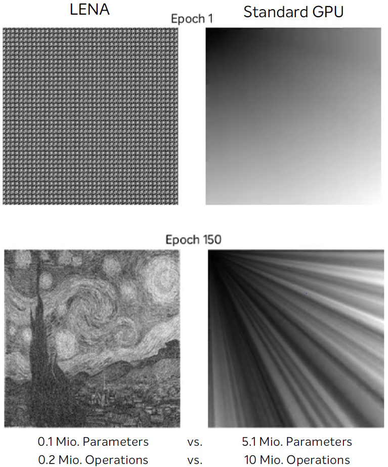
Well, this certainly looks spiffy, but just how good is this technology? I’m glad you asked because Michael shared an image that “gets the idea over” in a very visual way as shown below.

LENA vs. Standard GPU (Source: Q.ANT)
Suppose we are trying to train an AI to recognize Starry Night by Vincent van Gogh. We are performing this training using a LENA based NPU vs. a standard artificial neural network (ANN) implemented on a traditional graphics processing unit (GPU)
The results after one training cycle (epoch) are presented on the top row. The results after 150 cycles are shown on the bottom row. It’s easy to see how much further advanced is the Q.ANT solution. Also worth noting is that LENA required only 0.1 million parameters and performed only 0.2 million operations, as compared to 5.1 million parameters and 10 million operations with the GPU.
Now that I have your attention, I’ll start by telling you the way things are today, and then I’ll tell you where I think things may go in the future.
The way things are today is that the TFLN NPU shown in the first image above is mounted on a raw slice of silicon substrate—basically, a silicon chip without any transistors. All this substrate essentially does currently (in addition to providing something to sit on, of course) is provide the other sides of the capacitors for the modulators (I think of this as a “bulk capacitor plate” that can be biased or at least be connected to ground). Also today, optical signals are conveyed in and out of this device using regular optical fibers.
What about the future? Well, first, I can envisage the lithium niobate layer being mounted directly on top of a fully-functioning silicon chip. In this case, we could use circles of metallization on top of the chip (the side touching the bottom face of the NPU) to act as the faces of the individual modulator capacitors, and we could apply a layer of conductor to the top face of the NPU to act as the “bulk capacitor plate.”
Second, as opposed to using optical fibers to present optical signals “horizontally” into the edge of the lithium niobate layer, we could use laser diodes fabricated in the silicon chip to transmit optical signals vertically up into the NPU’s low-loss optical waveguides. Similarly, rather than using optical fibers to access optical signals coming out “horizontally” from the edge of the lithium niobate layer, we could use photo-diodes fabricated in the silicon chip to receive these optical signals vertically from the NPU’s low-loss optical couplers.
Imagine taking any of today’s high-end CPUs, GPUs, FPGAs, or SoCs that are currently silicon-only, and augmenting them with optical NPUs as discussed above. Everything would be presented in the same package (no bigger than today’s packages), looking just like regular chips to the outside world. I should note that all this is just idle speculation on my part; it’s not something Michael said Q.ANT was doing, but it is something I would be looking into if I had anything to say at Q.ANT.
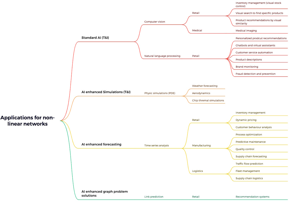
The potential applications for non-linear networks that could be enhanced with Q.ANT’s technology—providing much higher performance while consuming a fraction of the power—are myriad, multifarious, and manifold. Some examples are shown below.

Example applications for non-linear networks (Source: Q.ANT)
I think this type of photonic processing could be extremely interesting efficiency-wise and performance-wise for anyone involved in AI and high-performance computing (HPC). Of course, it’s not all about me (it should be, but it’s not). So, what do you think about all this?


One thought on “A Bold New Twist on Optical Computing”