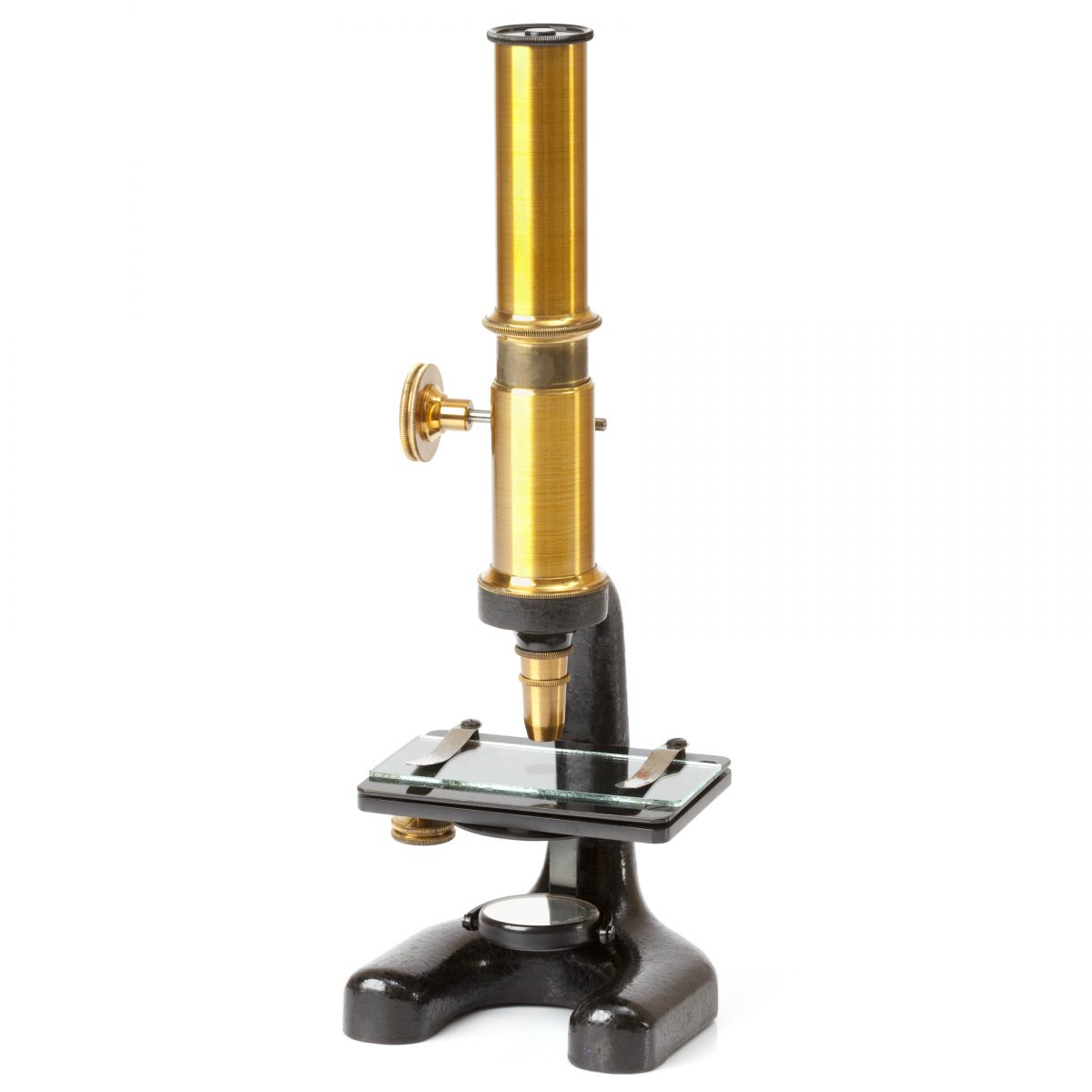
“Knowledge Is Good.” – Emil Faber, founder of Faber College
Data is good. So more data is better. Better enough to spend $3 billion, if you’re running ASML.
Advanced Semiconductor Materials Lithography (ASML) is the huge Dutch-based corporation that makes many of the shiny clean-room machines that produce your chips. You could say the company is big in small. But bigger can always get better, right?
Last week ASML announced that it was acquiring Taiwan-based Hermes Microvision Inc. (HMI) for about $3 billion, all in cash. That’s a major outlay, no matter what kind of business you’re running, and HMI is hardly a household name to most people outside of the semiconductor business. It’s especially expensive considering that HMI reported only about $200 million in revenue last year, which is less than 3% of ASML’s sales volume. So what could HMI have that is so valuable to ASML?
An invisible ray gun, as it happens. HMI has developed electron-beam technology that can resolve extremely small details, even by semiconductor standards. Their stuff isn’t used to fabricate chips, but to inspect them as they come off the production line. HMI is what’cha call a metrology company. They measure stuff. Really tiny stuff. And tiny is big.
You see, fabricating chips involves more guesswork than the chip companies would like to admit. There’s a lot of trial-and-error black magic involved. We’re dealing with feature sizes far too small to see, or even to measure accurately, and production volumes that make it impossible to inspect each and every chip. We’re long past the point where we can simply draw straight lines on the photomask and expect to see matching lines on the chip. Instead, we have to play games with masks, shadows, interference patterns, light sources – and even gravity! – in order to trick the equipment into producing the patterns we want. It’s all very bleeding-edge and counterintuitive. Statistics, Gaussian distributions, probability, data sampling, and closed-loop feedback mechanisms all play a big role in producing chips that actually work. And you thought this stuff was science!
It is science, but it’s science that’s right on the hairy edge of what we can control. Making submicron scratches in silicon is tricky business, so anything you can learn about the chip features that actually come out of your shiny machines is potentially lucrative knowledge. Improving silicon yields (the ratio of good chips to bad chips) by even a few percentage points is money in the bank. Knowledge is power.
(Background for software types: Almost all chips today are made using a technique called photolithography (Greek for “writing on stone with light”) because they shine a beam of light through a mask to make to make shadow patterns on the silicon. The details change over the years, but it’s still all lights and shadows. Electron beam, or e-beam, technology points a narrow ray of pure electrons directly at the silicon chip, like a lightsaber carving patterns in the sand.)
HMI’s specialty is e-beam metrology. That is, they measure stuff using a focused stream of electrons rather than the usual optical methods. The company was founded back in 1998 by former KLA-Tencor employees who felt that e-beam inspection held longer-term promise than the current optical methods. KLA (and most other tool makers) preferred to stick with their optical technology, while HMI quietly built up a lead in the e-beam world. HMI eventually became the de facto leader in e-beam inspection tools, almost by default. The company doesn’t sell a whole lot of equipment (see the $200 million number, above), but it is very profitable, with about 37% gross margin last year.
Theoretically, e-beam is great stuff. The technology can be used for inspection, as HMI does, or it can be used for fabrication. Focused electron energy can resolve much finer geometries than even the most advanced multi-patterned optical technology, sometimes by an order of magnitude. It’s essentially a scanning electron microscope (SEM), like you’d see in a physics or chemistry lab. In fact, you can even buy conversion kits to turn your SEM into an e-beam tool.
So the upside for e-beam looks very rosy. Indeed, it might be absolutely necessary if the industry is to ever move beyond the 10nm node, where future optical technologies appear to hit a wall.
What’s the downside? It’s achingly slow. Optical tools are much faster, even if they’re not as accurate. And in this business, productivity means profit. The nature of e-beam equipment is such that it can only inspect or fabricate one chip at a time, and that’s killing e-beam’s economic viability. The proposed solution is to use multiple e-beams at once in the same machine, but that turns out to have its own spooky, quantum-effect problems. In short, everyone knows that multi-beam is the way to go, but nobody’s figured out the secret to making it work reliably – if that’s even possible.
That’s going to require some serious R&D, and serious R&D costs serious money. HMI probably doesn’t have that kind of cash… but ASML does. By funding HMI’s presumed multi-beam efforts, ASML can extend its lead in this key technology, while simultaneously snatching it from competitors’ hands.
Meanwhile, back in the fab… We have a situation where the chips coming out of the fab don’t look like the design that went in, because of the weird nature of optical lithography and the strange behavior of very short wavelengths of light. This makes your feedback loop vitally important. As long as you can correlate inputs to outputs, you can eventually arrive at a solution that produces the desired output – even if you don’t wholly understand why it works. “Hey, if we do this, then the chip does that.”
Next, you need good mathematical models. Since all of this stuff is (theoretically, at least) controlled by fixed laws of physics, it should be possible to model all of this behavior and predict what will actually happen with some degree of accuracy. But that’s like predicting the weather. Sure, they’re both physical phenomena, but that doesn’t mean that they’re easy to model or well understood. Hence the need for more and better feedback.
What HMI’s metrology equipment allows ASML to do is to get better feedback on what comes out of the latter’s production equipment. That allows ASML to adjust its mathematical model of the chip design, which in turn is fed back into the lithography equipment to tweak its design parameters. The closed loop becomes a bit tighter, production cycles get a bit shorter, yields improve a little more, and everyone in the bunny suits gets a bit smarter about this funny business of making chips.
Quality guru W. Edwards Deming said, “If you can’t describe what you are doing as a process, you don’t know what you’re doing.” That pretty well sums up ASML’s strategy here. The company is spending some serious coin to better monitor and measure the exquisitely fine details produced by its own production equipment with the goal of feeding that information back into its models. The company calls this “computational lithography.” They’re basically calculating what the photomask should look like, regardless of what the squishy human designers think.
More importantly, if this works right, ASML should be able to predict what changes might be required to a design before it enters production, rather than tweaking it after the fact. It’s predictive, rather than reactive, feedback.
The acquisition comes at a good time for ASML. The company has spent years developing its newest extreme ultraviolet (EUV) tools for 7nm production, and they feel that they’re just about ready for prime time. But you can’t make 7nm chips if you can’t inspect them, so the success of one depends on the other. Since HMI is the largest (indeed, one of the few) companies making e-beam inspection tools, they were the obvious candidate for acquisition. So, in addition to improving the yields of ASML’s current photolithography equipment and bolstering its computational modeling expertise, the HMI deal may help to jumpstart sales of ASML’s forthcoming EUV equipment as well. That package of benefits ought to be worth, oh, I’d say, about $3 billion.


Multi-beam SEM silicon chip images like this one?!
http://bit.ly/29vX4sV