The semiconductor industry is ramping up for the wider adoption of 3D ICs, which promise better performance, reduced power, and improved yield. While some aspects of true 3D ICs are still evolving, solutions for testing 3D ICs are ready today. The test strategy for 3D ICs has two goals: improving the pre-packaged test quality and establishing new tests between the stacked dice. We describe a test strategy for 3D ICs based on a plug-and-play architecture that allows die, stack, and partial stack-level tests to use the same test interface, and to retarget die-level tests directly to the selected die within the 3D stack.
The fundamental requirements of a test strategy for 3D ICs are the same as for traditional ICs—portability, flexibility, and thoroughness. Therefore, we use an IEEE 1149.1 (JTAG) compliant TAP as the interface at every die and IEEE P1687 (IJTAG) networks and definition for test access. The test interface at each die is based on an IEEE 1149.1-compliant TAP because this is the most common standard device DFT interface. The same TAP structure is used on all dice, so that when doing wafer test on individual dice, even packaged dice, the test interface is through the same TAP without any modifications.
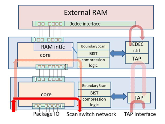
When multiple dice are stacked in a 3D package, only the TAP on the bottom die appears as the test interface to the outside world, in particular to the ATE. Each TAP accepts a special instruction to enable the next-level TAP in the stack. From outside of the 3D package, for board-level test for example, the 3D package appears to contain only the one TAP from the bottom die (Figure 1).

Figure 1. Overall architecture of a 3D IC test solution. A test is managed through a TAP structure on the bottom die that enables the TAPs of the next die in the stack and so on. A JEDEC controller is used to support interconnect test of Wide I/O memory dice.
Each die also uses IEEE P1687 (IJTAG) to model the TAP, the test access network, and test instruments contained within the die. IJTAG provides a powerful means for the test strategy to adjust to and adopt future test features. It is based on and integrates the IEEE 1149.1 and IEEE 1500 standards, but expands beyond their individual possibilities.
Improving Pre-Packaged Die Test Quality
An interesting benefit of 3D ICs is improved yield. Silicon area is a key factor in determining yield; the larger the die, the more likely it contains a fabrication defect. With 3D ICs, the functionality that would otherwise require a large die is segmented into multiple smaller dice that are individually tested before being packaged together. A defective (small) die can be detected and discarded before final stacked package assembly. Thus, only one of the multiple smaller dice would be discarded instead of the entire single large one if it weren’t segmented. Because the consequences of having a defective die in the stack are so large, thorough die-level test is very important.
Die tests include memory BIST for memories, embedded compression ATPG and logic BIST for logic, and die IO test. An important feature of memory BIST is to be “soft-programmable” so algorithms can be selected and/or programmed as needed based on what is learned during production. For logic test, a good option an integrated embedded compression ATPG plus logic BIST strategy that uses common test logic for both functions. ATPG provides an infrastructure for standard stuck-at, transition, and path delay tests, as well as newer high-quality tests such as timing-aware, cell-aware, and other specialized types of test. The logic BIST part allows for in-system test that is particularly important to ICs for automotive or medical applications.
The die IO test interface is based on IEEE 1149.1 boundary scan. Bidirectional boundary scan cells are located at every IO to support a contactless test technique known as “IO wrap.” Figure 2 shows an example of how IO wrap test works. Using boundary scan logic like this enables test at the die level, of the partially packaged device, and of the interconnect between packaged dice. The TAP and boundary scan logic perform an infrastructure test and a wrap test on each boundary scan cell IO. A contactless leakage test is also included; the die IO can thus be tested for excess leakage during wafer and other tests through contact with only the TAP signals.

Figure 2. Contactless test include IO wrap test and contactless leakage test. Bidirectional boundary scan cells are used to set a logic value, tri-state the driver, then capture the input to check that excessive leakage didn’t occur and capture a 0.
Reuse Die-level Test on 3D Stacks
3D ICs are a perfect application for using hierarchical DFT methods. Rather than generating ATPG test patterns at the end of the design cycle, you can complete most of the DFT insertion and ATPG on individual blocks/chips as they are ready. Then, software tools help you map the core-level ATPG and BIST patterns to the top-level design and retarget the test patterns automatically. Retargeting allows patterns that were created for an individual die to be retargeted to the 3D IC. In fact, the DFT logic and patterns for any die can be retargeted to any package in which the die is used. Thus, if the die were used in multiple packages, then only one DFT insertion and ATPG effort would be necessary, which would then be retargeted to all the platforms where it is used. Hierarchical test offers improvements in DFT efficiency, saving workstation memory load and reducing both ATPG runtime and overall test time for a more predictable schedule.
Test External DRAM
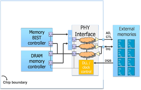
The most common use of 3D packages today is for external memories stacked on logic dice. The memories are usually DRAMs that follow a standard protocol. One test interface that we developed accesses external Wide I/O DRAMs through their JEDEC standard functional pins. The 3D IC memory BIST includes the physical interface logic (PHY), and is located within the logic die, next to the memory controller and right before the PHY and its associated external memory, as shown in Figure 3.

Figure 3. 3D test for external memory involves BIST logic being placed on the logic die that interfaces to the memory. The BIST logic is located at the physical (PHY) interface to the memory.
An advantage of using external memories in a package is that memories from different vendors can be swapped for cost or quality reasons (a.k.a. “second-sourcing”). The second-source die should still perform fine in the 3D package if it follows the same standard, such as Wide I/O. The memory pinout and operation will remain the same across different vendors. However, the internal physical layout of memory cells could vary. In those cases, you can use a pseudo-random data algorithm during memory BIST test that detects neighborhood pattern-sensitive faults (NPSFs) when the physical layout of the memory is unknown. You can load new algorithms into the soft-programmable memory BIST controller in case more targeted tests become necessary; there is no need to modify the design.
New Tests Between Stacked Dice
After ensuring high-quality die-level test, the second main requirement for a 3D IC test methodology is to test the interconnections between the stacked dice in the assembled 3D package. Our strategy is based on the boundary scan bidirectional cells at all logic-die IO, including the TSVs, that enable the contactless IO wrap and leakage tests mentioned earlier. Test is managed through the TAP and a JEDEC controller supports interconnect test of Wide I/O memory dice. We use IJTAG to define the boundary scan network and generate tests.
To validate the assembled 3D IC, an ordered test suite must be followed. This test sequence verifies the 3D IC starting with the simplest tests first, as basic defects are more likely to occur than complex ones. It then progressively increases in complexity, assuming the previous tests passed. The sequence is given in detail in our whitepaper “Plug-and-Play Test Strategy for 3D ICs.” [http://www.mentor.com/products/silicon-yield/techpubs/download/?id=82511&cmpid=8955]
After all the tests pass, all key parts of the packaged SOC and Wide I/O memory device are verified. Since tests were gradually applied in an orderly sequence, they all rely on previously-tested good logic, so detected faults are confined to the newly-tested part of the 3D IC device.
The test strategy we’ve outlined here will work today, but 3D IC test standards, test requirements, and the types of external memories being used are still evolving. It is this need for flexibility that led us to use IJTAG to structure our test architecture. IJTAG supports existing standards and related hardware, such as IEEE 1149.1 and IEEE 1500. Its broad definition also enables it to support many flavors of TAPs, BIST logic, and other DFT structures. It is this plug-and-play flexibility that makes a compelling and effective 3D test strategy.
—————————————————–
Ron Press is the technical marketing director of the Silicon Test Solutions products at Mentor Graphics. He has published dozens of papers in the field of test, is a member of the International Test Conference (ITC) Steering Committee, and is a Golden Core member of the IEEE Computer Society, and a Senior Member of IEEE. Press has patents on reduced-pin-count testing and glitch-free clock switching.
Dr. Martin Keim joined the Silicon Test Solutions group of Mentor Graphics in 2001, where he is currently Engineering Manager of the Memory Built-In Self-Test team. He is an active member of the IEEE P1687 working group and was editor of the sixth edition of the Microelectronics Failure Analysis Desk Reference Manual, responsible for the test and diagnosis chapters. For several years, Dr. Keim has worked on the organizing committee of the International Symposium for Testing and Failure Analysis, for which he will be General Chair in 2016. He holds several national and international patents and is author of many technical publications. He received a doctorate in Informatics from the Albert-Ludwigs University in Germany.
Etienne Racine is a technical marketing engineer for the Silicon Test Solutions products at Mentor Graphics. He has 15+ years of board- and chip-level DFT experience and has spent most of his career working on advanced BIST for memories and mixed-signal cores.


What do you think of Mentor’s 3D IC test strategy?