There’s been lots of discussion of the silicon interposer as a way to ease us into the world of 3D-packaged ICs. The silicon interposer is the main enabler for what’s typically referred to as 2.5D packaging; it acts like a high-quality micro-PCB that can be built using the silicon manufacturing infrastructure that’s already in place.
But silicon has some downsides. It’s an expensive interposer (even though we’ve seen that, paradoxically, some extra expense can lower overall costs), and it has relatively low resistivity, which affects how much neighboring signal traces might accidentally exchange unintended messages. Conveniently, silicon has a closely-related sibling that also figures heavily in standard IC production: SiO2. AKA, glass. It has higher resistivity, and so it could perhaps compete as an interposer material.
Glass interposers have been studied before, but, according to TSMC, only at relatively “high” thicknesses, down to 175 µm. (I know, it’s hard to use the word “thick” and such tiny numbers in the same sentence.) The via size and pitch in these prior experiments were 35-45 µm and 50-100 µm, respectively. TSMC’s current study used much thinner glass: 50 µm, with via size/pitch of 25/45 µm.
Atypically for TSMC, they provided a fair bit of information on their study in an IEDM paper. They describe a straightforward process (Figure 1) whose first step is the most critical: fusion-bonding a thick glass wafer onto a silicon carrier wafer. The catch here is that the bond has to be “void-free” to prevent glass cracking during the subsequent thinning process. Perhaps the reason why TSMC could be so generous with some of the information is that they were completely mum on how the void-free bonding was accomplished.
Once bonded, the glass is thinned down to the desired thickness, 50 µm. Vias are drilled using lasers and are then filled with copper, the excess of which is removed using standard CMP.

Figure 1. Simplified schematic of glass interposer fabrication.
Note that these are 300-mm wafers. In other words, this isn’t some lab-sized experiment – we’re talking large wafers, which makes sense if this is ever going to be used in a standard fab.
This process description leaves out an interesting detail: how metal traces are built. For some of what we’re going to look at, it’s obvious: after the above steps, you proceed with a standard metal layer, using photolithography to establish the geometries. But what’s missing here is how the bottom layer of metal is implemented.
The drawing above shows vias being drilled – to what? They say it’s just glass on silicon. Where are the underlying metal traces that these vias connect? Never mentioned. Perhaps that’s another trade secret. So I must speculate on the options.
- One approach might be that the silicon carrier wafer can first be patterned with metal before the bonding occurs. How that affects the void-free requirement isn’t obvious to me. It also creates an important alignment parameter when the vias are drilled and any other on-glass features are built: they’d have to be aligned precisely with the underlying patterning on the silicon wafer.
- Another possibility would be that the glass is bonded to one carrier wafer and then patterned with metal on what will be the bottom side before being debonded and transferred upside down to the second carrier wafer, after which thinning occurs. Such a process would alleviate silicon-wafer-to-glass-wafer orientation and alignment concerns, but it would still provide a void-free challenge.
- The other option, of course, is to do multiple glass layers. That is, to some extent, inconsistent with the process figure, which shows vias being drilled to the silicon side, but perhaps that’s a head-fake on TSMC’s part. If this were the way it was done, then the bottom glass layer would never have vias; it would always be the second (or higher) layer with vias.*
Interposer performance was judged by three different components: a 2D spiral inductor, a 3D helical inductor, and a high-speed transmission line (HSTL). Q is the critical figure of merit that they used to compare glass against silicon. Applications for such a system include cellphones, so RF characteristics in the few-GHz range are of particular interest.
The 2D inductor is laid out on one layer (Figure 2). The layers were 4 and 8 µm thick; line width and spacing were both 20 µm.
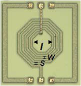
Figure 2. 2D spiral inductor
Whether done on silicon or glass, the resulting inductances remain equal until around 3 GHz. At that point, silicon starts to take a dive while glass provides increasing inductance with frequency. In fact, the silicon version actually becomes a capacitor at 8 GHz (Figure 3).
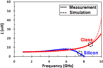
Figure 3. Spiral inductance vs. frequency for silicon and glass.
But what about the quality of the inductor? The Q of the silicon version peaked at around 18; the Q of the glass version topped out at about 30. The high-quality regime of the glass version also covered a better frequency range than did that of silicon (Figure 4).
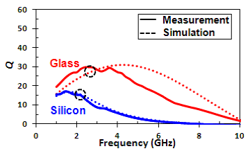
Figure 4. Inductor Q vs. frequency for silicon and glass.
The 3D helical inductor resembles a needlepoint project that your grandmother might have done. See? Who says those knitting lessons were a waste? (Yes, before anyone yells, I know that needlepoint and knitting are different…) Vias and lines combine to create one helical coil, the dimensions of which are determined not only by the metal layout, but also by the glass thickness.
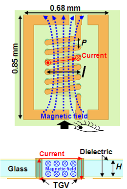
Figure 5. 3D helical inductor – top and side views.
Both inductors can have their inductance changed by altering the number of turns and the lateral dimensions. But because the 3D inductor also has the glass thickness as an adjustable knob, it’s possible to monkey with the value of an inductor without changing the lateral inductor footprint. That can help to keep area down. It also turns out that thicker glass means a higher Q (Figure 6).
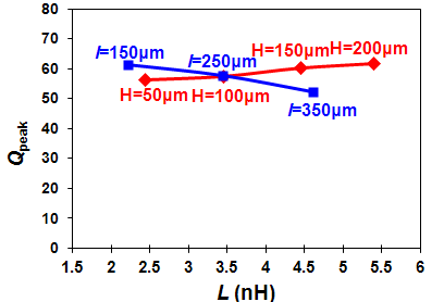
Figure 6. Peak Q vs. L with varying diameter (l) and glass height (H) for spiral (blue) and helical (red) inductors.
The catch is that you can’t change the glass thickness only for the inductor: once you establish a glass thickness, the entire interposer will have that thickness. So it’s an available knob, but one that affects more than just one inductor.
In general, the helical inductor outperformed the spiral one, saving area by 45%, increasing Q by 86%, and reducing the power dissipation ratio by 58%.
Finally, the transmission line. This test feature interconnected a WiFi baseband IC with its RF companion IC. They created it as a coplanar waveguide (CPW; Figure 7). Loss was more than 60% better than the silicon equivalent, and the eye opening was 85% better.
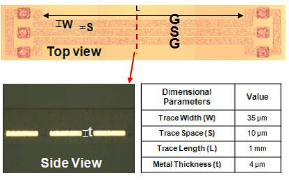
Figure 7. Coplanar waveguide creates an HSTL. G is ground; S is signal.
So let’s review:
- The glass version of the spiral inductor outperforms silicon.
- The helical inductor outperforms the spiral one.
- The glass HSTL outperforms the silicon version.
Um… is there any downside here? The results suggest that, from an electrical standpoint, glass is better in all regards. But there is a catch: thermal. Silicon conducts heat better, so glass could be an issue where heat dissipation is important (like under a power amp). The thinner the glass is, the lower the thermal resistance will be, providing better cooling. In addition, the denser the via grid, the lower the thermal resistance – for the obvious reason that the vias are acting as thermal pipes. (Which would provide a rationale for vias on the bottom layer in option 3 above even if there were no metal to interconnect between the silicon and glass.)
But there’s one other underlying assumption here that’s not really made explicit in the paper; I had to ask in the hallway to confirm. Often, when manufacturing something with a carrier wafer, that wafer acts simply as a manufacturing handle, to be removed once fabrication is complete. Like the falsework built around a bridge or arch, it comes down when work is finished.
But if that were to be the case for this, you’d remove the carrier wafer at the end to isolate the interposer. And that interposer would be only 50 µm thick. I mean, geez… I’ve got glass cabinet shelves a quarter-inch thick that I’m afraid of overloading. I can’t imagine even breathing near a piece of glass that thin.
When I asked, the presenter confirmed (somewhat coyly) my suspicion that you could leave the carrier wafer on for strength. Unless you’re doing multiple layers, in which case each higher layer could be thinned on its own carrier, after which it could be debonded (details not disclosed) and transferred onto the stack, with only the lowest level remaining attached to its carrier.
That attached carrier wafer will help to explain why thinner glass provides better thermal performance: if the glass is thin, then the heat has less far to go before moving into the silicon carrier wafer, where it can be shunted away more easily.
If you have the IEDM proceedings, you can find more detail on this study in paper 13.4.
All figures courtesy IEDM.
* I’d ask the author, but, with conference papers, once the event is over, it’s almost impossible to get any follow-up contact… and this question, which seems obvious to me now, didn’t occur to me until too late…




What do you think about glass as an interposer?