

A simple, straightforward EDA whitepaper recently got me asking some demographic questions. The answers say something about where analog and digital designs are being done – and where they’re coming together. (And yes – sorry, but the Internet of Things (IoT) is involved.)
Whitepapers are popular these days. Nothing new about the whitepaper concept, but how many of them get written during a given period of time (shall we call it the “whitepaper density”?) varies with the economic cycle. And the density is high at the moment.
Whitepapers can be a really useful way to get a technical message out without it sounding like marketing – if done right. You can talk about your product, unlike in an editorial article. But if you keep the tone analytical and professional, it doesn’t come across as marketing. You hold back on the, “OUR PRODUCT EFFING ROCKS” enthusiasm. More like, “Given these numbers and the trends in the industry, there’s a high likelihood that our product would be perceived as effing rocking.”
Which would also suggest that whitepapers are most useful for new concepts and new solutions. Which is why I was surprised to see a whitepaper put out by Tanner (now part of Mentor) on the topic of: PDKs.
Because PDKs aren’t new. (Even if you think they effing rock.)
I read through the whitepaper, and it was straightforward: here’s what’s in a PDK, and, in particular, here’s why analog p-cells are different from digital standard cells. All well and good – I can always use a brush-up. But… why now?
There are two possible reasons: either they’re clueless about topic and timing (not something I would expect of Tanner) or they’re seeing something that we’re not seeing. So I checked in with them to understand better who the target audience for this whitepaper was.
The first part of the answer made academic sense, but it still wasn’t satisfying: it’s an increase in analog and digital coming together – the AMS (analog/mixed signal) thing. All well and good, but that’s not new either.
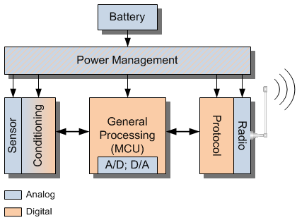
I wondered whether this reflected an increase in the amount of general analog circuitry out there. But that’s not really the case. Yes, IoT edge nodes, for example, could be said to have more than their fair share of analog: they sense the world; they convert that to digital; and then, if wireless, they radio the results back home. And they do that on a stingy power budget.
If lots of these nodes get shipped, then yes, there’s more analog out in the world. But much of that could simply reflect large volumes of the same circuits. It’s not clear that there are huge numbers of new analog designers coming on board. And, indeed, that’s also not what Tanner is seeing.
Turns out that their intended audience was digital engineers that are starting to hit on the fringes of analog circuits more and more. In particular, for circuits involving both new analog and digital elements. It’s not about more analog engineers; it’s about more digital engineers having to work with analog.
I still wanted to understand what’s driving this. Two common, long-standing analog domains have been radios and the analog peripherals on microcontrollers (MCUs). Tanner confirmed that they’re pretty well established, and, while work continues on these, it’s incremental, for the most part – making the receiver that much more sensitive or transmitting more data with less overall energy consumption.
If we stick with the IoT edge-node model, that explanation accounts for two out of the four analog islands: the MCU and the radio. The two remaining islands are power management and sensor conditioning. The latter is, in particular, where Tanner is seeing demand for this basic analog remedial education.
Sensors obviously measure analog phenomena. The question is, at what point – if ever – do you digitize? Some sensors never do – they provide analog outputs. So the analog circuitry is all about providing a clean, stable, reliable signal. But it’s all analog work – no digital designers are poking their noses in here.
Many of the higher-volume sensors, however, not only digitize their outputs; they even do additional abstraction work so that the sensor provides higher-level outputs. Not just an analog value representing acceleration, but full orientation. Not just orientation, but mode of movement (Running? Walking?) and number of steps.
All of that high-level stuff would ordinarily be done in an MCU outside the sensor. Now it’s done inside the sensor package – very possibly using an MCU. Which makes the highest-level abstraction a story more about integration than the analog/digital boundary.
No, other than sensors with analog outputs, most sensors still live by the compulsion to digitize analog signals as quickly as possible and then do further work. But the exact position of that border can move around. This is the realm of “signal conditioning,” where you’re taking a rickety, shaky analog signal and removing some of the noise and perhaps linearizing what’s inherently a non-linear phenomenon and then maybe scaling the results to give greater precision.
Do you do these things in analog or digital? Some of these could be pushed back and forth across the divide; this is a big part of where Tanner sees digital engineers encountering analog – and benefiting from some basic background on the p-cells in PDKs.
There is perhaps another area where this phenomenon could occur, and it relates to the final remaining island in an IoT edge node: power management, and, in particular, energy harvesting. Looking at the circuits presented in leading-edge conferences like ISSCC, there’s tons of analog there. Problem is, that’s still a research area, so there’s not yet a lot of activity integrating energy harvesting into commercial product. Current power management relies much more on tried and true battery-based technology. As with radios, there’s lots of tweaking going on here to provide better power management at lower energy cost, but it’s relatively more stable.
So, no, PDKs aren’t new. And there doesn’t seem to be a demonstrable change in the amount of analog design going on, but Tanner is seeing more digital engineers having to confront analog stuff. And, in the end, they see that originating to a large extent out of sensor companies.
And yeah, I do grimace a bit myself – jeez, does everything reduce to an IoT discussion? Thankfully, no, but the IoT does promise a robust new high-volume market if the hoopla is validated. Which means… we’re going to keep coming back to it either until it’s not news anymore or until it fades and we move on to something else.
More info:


Are you a digital designer brushing up against analog? What are you working on?