What follows is something I enter into with great trepidation. Getting this… article thing… to a point where you can read it has involved more brain cell abuse than I inflicted upon myself during my entire college career. OK, it sort of feels like that, anyway.
We’re going to talk about double-patterning. Yeah, I know, we’ve talked about it before and it wasn’t so bad, was it? Ah, that’s because there isn’t just one double-patterning: there are two. Actually, there are more than two, but most of the other major variants don’t seem to be finding their way into production, so we’re going to ignore them. Denial being an awesome tool when used the right way.
And even the two remaining ones have lots of minor variants, but we’re not going to delve into all of those. Because those minor variants are nothing compared to the major distinction between the two approaches. In fact, having tried to bend my brain around this thing, I am now convinced that these are like fraternal twins – and one is benign and the other is evil.
I’ve been guided through this with the help of the folks at Mentor and, in particular, David Abercrombie – who has thankfully (and not condescendingly) agreed that this stuff can be maddening. And if he thinks it is, then I don’t feel like quite such a wuss.
The double-patterning we’ve seen before is the good twin, and it goes by the name “LELE.” (It’s pronounced “ellie elllie,” not “leh leh.” Just to be clear.) That stands for “litho-etch; litho-etch.” In other words, it’s simply two standard litho steps, one after the other. Expose and etch half the pattern; then do the bits in between. Easy peasy.
Problem is, when you’re aligning that second mask, you have to be damn sure that you’ve aligned it smack dab over the prior mask. This “overlay” challenge has enough people concerned that they’ve gone down to the cage in the basement to fraternize with the evil twin.
And the evil twin is SADP. (Personally, I’d have stopped after the D. Seems more accurate.) This stands for “self-aligned double-patterning.” Or “sidewall-assisted double patterning.” See? Not even the professionals can agree on what to call it.
The thing is, this stuff isn’t just theoretical. It’s not something that your friendly neighborhood EDA company can abstract away in a tool so that you can mosey along in blissful oblivion. If you’re a chip designer, this one may affect you – and exactly how it will affect you isn’t even a done deal; it’s still being debated.
So what I want to do here is to split this discussion up into two pieces. In part 1, I’m going to describe what SADP is (or at least one variant of it), contrasting it with LELE. There will be new vocabulary words. You did bring flash cards, right? In part 2, we will look at what “coloring” means in SADP and what some of the EDA and design challenges are.
About a year and a half ago, I opined that a fundamental change in chip design is that masks look less and less like what it is you’re trying to pattern onto a wafer*. LELE is somewhat like that – each mask contains only some of the features – but it’s not a big mental leap to superimpose them. SADP, on the other hand… yeah… well, we’ll go through a simple example and I will try to leave you begging that we don’t go through anything harder. (And if I don’t succeed, then I will beg you not to make me repeat it with anything harder.)
Before we dive in, by the way, you do know that folks are talking about triple and quadruple patterning, right? From what I’ve seen, those seem to be akin to the simpler variety, like LELELE for triple patterning. I’m sure some sadist somewhere is trying to dream up a harder way to do it, but we won’t go there. (For as long as we can avoid it.)
Quick review of the problem
Why was it again that we’re doing all of this? Because we want to bring features closer together than current 193-nm immersion lithography will allow. Heck, by all rights, we shouldn’t even be doing the things we are currently doing, but smarter people than you and I (well, I anyway) came up with things like optical proximity corrections (OPC) and design-for-manufacturing (DfM), which essentially pre-distort masks so that the distortions of the pre-distortions end up looking like we want them. Which has required some serious understanding of how the distortions work.
But we’re running out of room on that. What we really need is a shorter exposure wavelength so that we can resolve smaller features, but that would be the realm of extreme UV (EUV), and… well… yeah; we’re all still waiting on that one. So we need to pull another trick out of our sleeve while EUV comes alive.
And that trick is double patterning. Which is easiest to understand with LELE. I’ll use a simple example to illustrate it, and then we’ll move on to the nasty stuff.
Those of you who have read my stuff for a while have probably noticed that I don’t use a lot of graphics. Well, today’s topic requires graphics – lots of them. And, frankly, I found that by forcing myself to draw my own graphics (rather than copy some from, say, a Mentor whitepaper), I also forced myself to confront stuff I didn’t understand until it made sense. So I recommend doing that.
LELE
LELE is simple in concept. You divide up your features into two sets. Let’s say we want to create the shapes in Figure 1. The problem is that the arrows show where these two things are too close together to be formed in a single exposure; they violate the spacing design rules.
By the way, one thing I’ve done with that figure is to show both top and side views. So many double-patterning discussions give you only one or the other, as if, given one, the other would be obvious. But I didn’t find that to be the case, and showing both together helped me, so I’m going to do that where I think it will help.
So what you see is the obvious top view, but then on the side and bottom I show the horizontal view (even though the one on the side is rotated 90°).
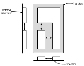
Figure 1. Desired features
To obtain this pattern using LELE, we simply do one feature in one exposure and the other in a subsequent one.
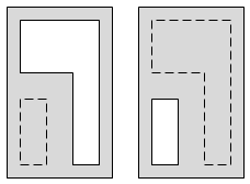
Figure 2. LELE masks.
Now you may well be aware that there are complications with deciding which features go on which masks and possible “coloring conflicts.” We’ve covered those before, so I won’t delve into them here. Conceptually, they’re not hard to understand.
And that’s all we’re going to say about LELE.
Into the dungeon
I’ve wrestled with how best to attack the SADP topic, and I’ve decided first to show conceptually how it works. In part 2, we’ll approach it from a different angle: how to arrive at masks that will yield a desired pattern. For the first part, we’ll use a trivial – yet useful (for fins, for example) pattern. For part 2, we’ll look at slightly more complex patterns. I’m not going to do anything harder than that because I frankly hate cleaning up the wall behind me after my brain explodes.
The conceptual part is important, because, as far as I can tell, this whole thing has come about due to some clever person(s) who figured out how to leverage a phenomenon that, up to that point, had been considered a problem: sidewalls.
This relates to what happens when you coat a surface with some kind of gunk, like a photoresist or other film. Assuming the surface isn’t flat, the gunk will conform to the ups and downs. And when you remove it by attacking from the top, as when etching, then you’ve got these funny artifacts that form around steps. Remember step coverage, when we were worried about voids? Yeah, it’s like that, only the opposite.
So in Figure 3, you see the green gunk that’s been deposited over two pink vertical features, and the layer conforms to that shape. Sort of.

Figure 3. Gunk layered over steps.
If we etch from above, then the surface will be removed at the same rate all over – including by the step discontinuities. If we etch to the point where we remove all of the layer from the flat portions, we’ll still have some residual gunk in the step corners. If we etch just a bit more, then we get this nice sidewall-looking thingy (Figure 4). Instead of being a problem, these are going to be useful. (I don’t want to over-represent how accurate these drawings are; I’m merely trying to cross that gap between how it looks before etching and the sidewalls as they’re usually drawn.)

Figure 4. Creating sidewalls.
Now we can remove the middle pink portions and we’re left with three gaps that are closer together than anything we could have exposed. We exposed the two outside ones, but the middle one was created by the sidewalls; we have effectively doubled the pitch.
![]()
Figure 5. Sidewalls double the pitch.
A bit of vocabulary here: the pink bits that we eliminated at the end have a special name: mandrels. Why? There’s probably some good historic reason. I haven’t found it particularly mnemonic of their function, but there you have it. (Perhaps someone reading this has the history and can comment below.**) Obviously the mandrel must be impervious to the sidewall etch and vice versa.
That’s the basic concept of how it works, but it can be applied a couple of different ways. And to understand better what’s happening, we also need to look at a top view of the process. So let’s assume we’re going to try to create the following pattern:
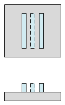
Figure 6. Desired pattern; middle feature can’t be exposed.
In this case, let’s make the blue material silicon. So this could be, for instance, three fins for FinFETs. I’ve shown the middle one with dotted lines because it can’t be exposed with the others; it’s too close to them. The outside features, on the other hand, can be exposed. I’ve shown the top and side views; I’m going to focus only on the one dimension, so I’m not going to worry about the other rotated side view for the moment.
So, to set this up, we expose two mandrels:
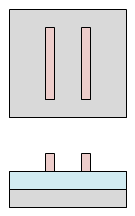
Figure 7. Mandrels deposited, exposed, and etched.
This involves depositing the mandrel material and then exposing and etching the pattern. (I haven’t shown those steps because they’re standard.) For those of you who already know this stuff, what I’m showing you is actually slightly incorrect, but it’s easier to visualize this way. I’ll come back to the problem at the end.
Now we can deposit the sidewall material:
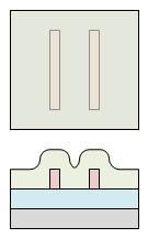
Figure 8. Sidewall material deposition.
The side view should look familiar, although now I’m showing the underlying silicon layer.
Now we etch down the sidewall material. I spelled out that portion in more detail before, so here’s the result:
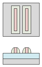
Figure 9. After sidewall etching.
And now we can remove the mandrels:
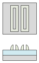
Figure 10. Mandrels gone; sidewalls remain.
Now you can see why the side-on view isn’t sufficient. From that standpoint, it looks like we’re done; we can use the sidewalls as a mask and transfer the pattern down into the silicon. But from the top view, you’ve got these sidewall rings. So now what? This is where a second exposure comes in.
It’s probably a good time to back up a second. We’re talking about double-patterning here; LELE clearly has two exposures, but when we looked at the basic SADP concept, there was only one exposure: when we laid down the mandrels. Doesn’t sound like double patterning.
But of course it’s not that simple. Now we need to clear away unwanted sidewalls, so we have a second exposure using what’s called a “block” or a “trim” mask. This is used to isolate only the areas of interest. The sidewalls are going to protect the underlying silicon from an etch. We want three fins, but we have four sidewalls. We also don’t care about the entire sidewall rings; we want only the one dimension. So we create a mask that blocks out the stuff we want. Note that this mask can tolerate a bit of registration error – and that’s why we’re bothering with this in the first place: to eliminate mask overlay sensitivity.
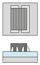
Figure 11. The “block” or “trim” mask.
With the mask/photoresist in place, we etch the rest of the sidewalls away, giving us the three sidewalls that we want:
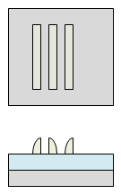
Figure 12. Final sidewall configuration.
We can now etch the underlying silicon to create fins. This is also referred to as “transferring down” the pattern since the sidewall pattern is transferred to the underlying silicon.
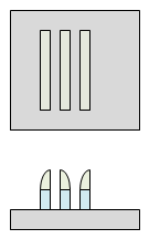
Figure 13. Sidewall pattern transferred to silicon.
And now we can remove the sidewalls and we have our finished result.
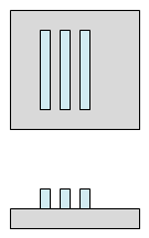
Figure 14. Finished patterned silicon.
Now… those of you paying close attention may notice that the pattern we’ve ended up with here doesn’t look exactly like what I wanted. It’s shifted over a little to the left. And this gets to that “mistake” I mentioned earlier. The intuitive way to approach this was to place the mandrels where we wanted the features, but the features weren’t patterned by the mandrels; they were patterned by the sidewalls, which are next to the mandrels.
And this gets to the trickier bit of SADP: deciding where to put the mandrels so that you end up with the pattern you want. And that’s going to be the topic of Part 2.
But one last note here. You can also reverse the “tone” of this process. Instead of creating features under the sidewall, you can create them in the gaps instead. This is used for etching oxide for filling with metal. If we take the sidewall pattern we created above, but assume it’s overlying oxide instead of silicon, we have the following:
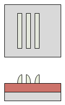
Figure 15. Sidewalls over oxide.
Now we etch the oxide to create trenches for metal… (yeah, I’m being lazy and neglecting the fact that the oxide on the far left and right would also be etched as shown… not relevant to the discussion…)
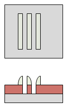
Figure 16. Trenches etched.
… and then we remove the sidewalls…
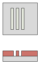
Figure 17. Sidewalls removed.
… and fill the trenches with metal.
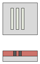
Figure 18. Trenches filled with metal.
In this case, the features do align with the original drawing we had, although there are only two of them instead of three (simply because I re-used the other example without going back to the beginning). This again gets to the question of how you decide what to put where. So the main point of this exercise was to show that you can use either the sidewalls or the gaps between the sidewalls to create your features.
Beyond that, I’ll give you a week and a half or so of rest, and then we’ll continue with Part 2.
*I just went back to that article and noticed one of the comments specifically calling out SADP as another example that I hadn’t mentioned in that piece. And… oh my… I just checked the profile of the commenter, and it’s none other than David Abercrombie.
**From Dictionary.com:
man·drel
noun Machinery
- a shaft or bar the end of which is inserted into a workpiece to hold it during machining.
- a spindle on which a circular saw or grinding wheel rotates.
- the driving spindle in the headstock of a lathe.
Origin:
1510–20; perhaps akin to French mandrin
Based on the Random House Dictionary, © Random House, Inc. 2013.


We’ve gone through the first layer of basics for SADP double-patterning. Are you with me so far? Comments or thoughts?
Good start Bryon! You’re a good student. Think of it like learning to solve the Rubix cube. With enough practice I’m sure we will learn to make it easy. You can bet that a lot of work goes on behind the scenes before a design rule manual and an EDA tool ever get handed to a designer. We do our best to take as much difficulty out of it as we can, but the more educated you can make yourself, the faster the learning curve and better the productivity.
What happened to Figure 8? Is it the same as Figure 3? Thanks
Look4me45, yes, it is. I just used Figure 3, which is simpler, to introduce the fundamentals of what’s happening. Figure 8 shows where this falls in the sequence of steps (and includes the underlying layers that I omitted for simplicity in Figure 3).