


Foreword by Kevin Morris
Have you noticed that there is no Moore’s Law for circuit boards? Sure, we have seen some gradual improvement in PCB technology over the past couple of decades, but we’re still pushing FR4 around pretty much the same way we always have, and the PCB is now a huge limiting factor in our ability to miniaturize our systems and make them more reliable.
Is it getting to be time to ditch the FR4?
Bob Conn is a fascinating guy – what many of us in engineering would think of as a “renaissance man.” We are excited to present the first in a series of articles by Bob about silicon circuit boards (SiCBs). Bob will take us through the practicalities of using SiCBs in the current world and give us insight in to how SiCBs may evolve as viable solutions for an increasingly large segment of our design work.
Enjoy!
-Kevin Morris
In the following series of articles, I’ll present a design of a silicon circuit board-based, high-performance computing (HPC) system capable of providing one petaflop of performance in one cubic meter. This series will cover a lot of technology, some history, and a fair amount of storytelling. It will be a do-it-yourself guide on how I would build 2.5D and 3D silicon systems using silicon circuit boards.
-Bob Conn
———————————————————–
The Condensed Guide to Silicon Circuit Boards
Silicon circuit boards (SiCBs) are similar to printed circuit boards (PCBs) but made with a silicon substrate rather than FR-4. Bare die and stacked 3D die are the intended components, as are any bumped packaged part. Silicon circuit boards can be made in almost any typical wafer foundry using either back-end-of-the line or front-end-of-the-line processing, depending on the foundry.
SiCB sizes fall between PCBs and integrated circuits (ICs). A typical PCB is 10 inches by 10 inches, a typical SiCB is 2 inches by 3 inches, and an IC is less than an inch on a side.
Silicon interposers, as distinct from silicon circuit boards, are generally reticle-limited in size – about 1 square inch – and are intended to go into a package. Silicon interposers often connect things that are specifically designed to interface with the silicon interposer – for example, the Xilinx silicon interposer connects 4 separate FPGA dice designed for the interposer. A number of vendors now provide silicon interposer fabrication.
SiCBs are not limited to a reticle in size. They can be the size of a wafer. They are more like small PCBs with dozens of components. Simply by removing the dice from the package and reducing trace sizes, it’s possible to turn a design based on a large FR-4 PCB into one on a small SiCB, which is less than one-quarter the size.
An HPC design on a SiCB may include 4 large FPGA dice and 8 or 16 memory dice, maybe a CPU die, some chip-scale-packaged oscillator/clock drivers, bypass capacitors, and I/O connectors. See Figure 1. This may be about 60mm x 70mm and less than 3mm thick – with components. Add a few more millimeters for heat sinks.
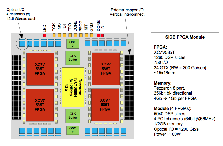
Figure 1. A 58mm x 68mm Silicon Circuit Board Intended for High Performance Computing
How I Started Researching SiCBs
I was working at Xilinx at the time that I started getting interested in SiCBs. We wanted to do huge SPICE simulations a lot faster. Often we had run times in months, so we were missing a lot of verification.
I figured I needed about 64 big FPGAs in order to run SPICE jobs approximately 100x faster than what we were able to do at the time. But 64 FPGAs and associated memory, regulators, etc., take up a lot of space – typically a 19” rack or several seriously large PCBs. Could I make it a lot smaller? I wanted to set it on my desk and do massive SPICE simulation work.
I shared this problem with two friends over beers at the Los Gatos Brewery. Since I was dabbling in stacking bare dice (configuration memory dice on top of an FPGA die) at Xilinx at the time, and the three of us had designed and built plenty of PCBs using packaged FPGAs, we thought we knew enough to connect a bunch of bare FPGA dice on a single wafer – maybe 8 or 16 – with a lot of memory dice.
The three of us had spent many years together doing prototype design and assembly work at Connsult and Xilinx, and we knew how to get things assembled and tested. By using a silicon wafer, we decided we could do all the routing out from under the FPGA dice in only 2 or 3 layers rather than the 6 or more layers on a typical FR-4 PCB. We knew the reliability would be better than with packaged parts (we had recently completed some reliability studies that supported this).
We also expected the I/O performance to improve. And if we stacked up 8 or so of these wafers, added some power regulators (on FR-4), connected some fans, and put it in a small box, I’d have my desktop supercomputer. And maybe I could build a few more for friends.
How to Design and Build a SiCB – An Overview
How to design and build an SiCB will take a few more words than this article. Each section will be a future article. For now, here are the highlights…
Design
Neither PCB layout tools nor IC layout tools are quite appropriate for SiCB design. Either will get the job done, and both have advantages and drawbacks. PCB tools are good at routing but need to produce IC output files (GDSII) and allow dimensions below a micron. IC design tools are mostly about area and don’t have the routing performance or the ease-of-use of PCB tools.
Assembly issues affect the design cycle. For example, what size of bumps are used and are they on the SiCB or the bare die?
Mechanical issues of connectors and attachment to a PCB need to be dealt with.
Acquire Tested Parts
Data sheets for bare dice are becoming available. However, it may take calling the factory to acquire one. Some memory houses (e.g., Micron) have bare die data sheets available online. These parts are fully tested in die form; however, not all bare dice are fully tested. Determining how much testing is needed and how to do it has some challenges.
Fabricate SiCB
SiCBs are fabricated with semiconductor IC fabrication technology. An odd thing happens here. World-class foundries are generally reticle limited (maximum imageable area) and can produce only silicon interposers or small SiCBs. For larger silicon circuit boards, reticle stitching is available. Or we can to look to older fabs that can do full wafer masking.
Typical copper metallization is 2 microns thick. Appropriate minimum feature sizes in SiCBs are around 5 microns. Traces that are much narrower than this are too slow for runs of several centimeters. (Interposer folks can use narrow traces because their runs may only be a few millimeters.) And these trace sizes are easily producible by the older fabs, so there are lots of potential vendors.
Other substrate possibilities include organics, ceramics, and glass.
Fabrication usually includes through-silicon-vias (TSVs) that are commodity processing today.
Assemble
SiCBs can be assembled by high-end PCB assembly houses. Good ESD control and automated pick-and-place machines are required when handling bare dice. Part assembly follows typical surface mount rules. Either the parts are bumped or the SiCB is bumped. Pad pitches of 30 to 40 microns are fine. Bare die underfill is not needed because of the reduced thermal/mechanical stress from matched temperature coefficients between the die and the SiCB.
Test and Rework
Using combinations of self-test, flying probe test, and modified package and wafer probing test fixtures, we can test assembled SiCBs. Typical PCB rework techniques are available to replace components.
Issues
How Do You Get Tested Parts? Known Good Die – KGD
Acquiring known “good-enough” bare dice is possible by several means. More chip houses are making bare dice available, but it does take some rooting around to find sources. And, more importantly, the first generation of silicon-to-silicon (never intended for a package) bare dice are available. These silicon-to-silicon bare dice can provide I/O power of less than 1pJ per bit. By eliminating the package, dice intended for silicon substrates are now being built with more than 2500 I/O pins, something not possible with packaged parts. Think of the memory bandwidth improvements.
Testing of bare dice and SiCBs to insure maximum yield is available. Sometimes the vendor provides KGD, and sometimes further testing is needed. There are many options here.
How Do You Get On and Off? Optical or Copper
One problem of SiCBs is their small size. It’s hard to imagine attaching a typical copper-copper connecter (e.g. CX-4, USB, etc.) to a 4” x 4” piece of silicon covered with bare dice and not have it instantly break the first time someone plugs in a cable. However, there are ways to provide mechanical support that can improve the SiCB ruggedness. 3D printers provide interesting options.
Optical I/O is preferred for high-band-width paths. And, optical connectors can be directly attached to SiCBs.
How Do You Get Power In?
Power distribution and routing have particular problems for high-powered bare dice (e.g., FPGAs and CPUs) because the large dice have been designed to rely on the package substrate to distribute power in millimeter pitch increments. Package substrates often have copper more than 15 microns thick to distribute power while SiCBs may be limited to 2 or 3 microns. One of several ways to dodge this issue is to use embedded power regulators – put transistors in the silicon of the SiCB.
How Do You Keep It Cool?
Cooling is with air, cold plates, or, in some cases, immersion. Good airflow management through a stack of SiCBs spaced several millimeters apart can handle 1kW in a volume 4” x 4” x 4”. Using cold plates, readily available today (and they don’t leak), makes the cooling job easier but heavier.
Features and Benefits
Reliability
Reliability is improved because temperature coefficients are matched – bare silicon dice on a silicon circuit board. An important driving factor in my interest in SiCBs is this inherent reliability improvement. When we talk of HPC, we need to talk about system reliability and what happens when parts of the system fail. An SiCB-based system has fewer parts and can be easier to re-work or repair than an FR-4 based system.
SiCBs also have fewer I/O interfaces because of the elimination of the package and the reduction in the number of thermal/mechanical stress points.
Signaling
On-SiCB signaling speeds are faster than on an equivalent PCB because the distances are shorter. Eliminating the package eliminates a substantial amount of parasitic inductance and capacitance. Because the wires are fairly small (2 microns by 8 microns, typically) they are somewhat resistive, and we have a wonderful – lossy – signaling environment, so termination of transmission lines is not needed.
EMI and radiated energy is reduced.
High speed signaling through a TSV costs a lot of signal integrity if they are much longer than 100 microns. There are many ways to dodge this issue.
Costs
Today, one can build a few dozen to a few hundred prototypes, depending on size, for approximately $75k, using world-class foundries such as TSMC, Global Foundries, etc. Shuttle runs are becoming available. New processes using laser ablation for patterning might make prototypes available for less than $25k. In future articles, I will write about a current project I’m involved in to make laser ablation processes available.
Low Power
Cooling needs are somewhat reduced on an SiCB compared to PCBs because the I/O power requirements have dropped significantly – in some cases I/O power is less than 10% of packaged part I/O power. Designing custom I/O for intra-SiCB connections can further reduce I/O power.
Many Links, But No Chain…Yet
The links of a supply chain for SiCB design, parts acquisition, manufacturing, test, assembly, and re-work, are all available. They are not yet connected together into an easily workable supply chain, but as the technology advances, these links will join together.
Futures
I never imagined I’d have to invent a new technology to build my little HPC system just so I could do some SPICE simulations, but here I am.
Future articles will look more in depth at the SiCB issues, how to build one, and how to build a 64-FPGA HPC system.
I welcome your questions and comments.
About the Author
Let me tell you a bit about myself. After living through the best time ever to go to school, I graduated from UC Berkeley in 1970 and started working as a design engineer at National Semiconductor, working on two-inch wafers with 10-micron feature sizes.
That led to 10 years of work at National, Fairchild, and AMI, followed by 15 years at my own design company, Connsult, doing all sorts of engineering and prototyping – robotic wafers handlers, portable parking ticket writers, a flight recorder for the Voyager aircraft, software architecture, RF ID tags, telecom central office equipment, etc. Then I spent 10 years at Xilinx and did the first 3D work there in 2001, and twice I was awarded the Ross Freemen Innovator-of-the-Year award. The last 8 years, I have been at Research Triangle Institute and UC Berkeley developing and designing silicon circuit boards.
I like working on difficult technical problems. I have more than 70 patents. I’ve won gold medals in rowing. My dad was a Pan American Airways manager, so I was born in Portugal and grew up on various Pacific islands. I’ve built my own airplane and two houses. I have two great boys and a happy wife. I live on Hawaii Island.
I’m looking forward to sharing what I have learned about silicon circuit boards and how I learned about it.
Bob Conn


Would you consider doing a design with a silicon circuit board?
The FPGA vendors are well underway with production designs that leverage the smaller “interposer”. I say smaller as we think of an interposer as being reticle limited in size whereas the silicon circuit board can be as large as the wafer.
My question is, since it made economic sense for the FPGA vendors to break up their larger designs into smaller die that assemble together on an interposer…shouldn’t it begin to make sense for the larger SoC designs out there? At some point it should make economic sense to break up very large SoCs as you can assemble things like analog and memory functions in separate die with their optimized processes onto an interposer or larger silicon circuit board.