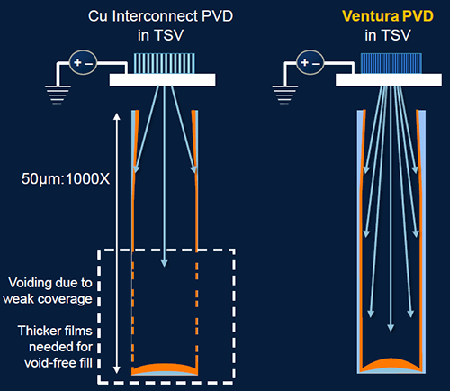
We recently looked at Applied Materials’ solution to the challenges of lining small vias: using cobalt. But those are through-dielectric vias. What about through-silicon vias (TSVs)? After all, they can be a thousand times deeper than a standard via, so if a standard via is hard to cover, imagine how hard it must be for a TSV.
Of course, we’re talking a wider via, but AMAT says that standard physical vapor deposition (PVD) tools do an inadequate job of coating the TSVs when applying the barrier, for lots of the same reasons we discussed in the cobalt story.
Their solution to the TSV issue isn’t quite as radical as a new metal; it involves tightening up the angle of dispersion for the metals, providing better coverage. With better coverage, the barrier can also be made thinner, saving cost. A thinner layer is faster to deposit, improving throughput (and reducing cost).

(Image courtesy Applied Materials)
In addition, they’ve built a production-worthy chamber for use with titanium rather than the more typical “proven” tantalum. Titanium apparently being cheaper than tantalum. Both can be integrated with the copper seed.
You can read more about their Ventura PVD in their announcement.


