


Two ongoing questions have plagued analog design for many years:
- How can we design analog circuits more quickly and more portably?
- How can we keep up with the growth in circuit size while still providing gold-standard sign-off simulation in a “reasonable” time? The meaning of “reasonable” being somewhat fluid…
At this summer’s DAC, I had a couple of conversations, each dealing with one of these questions. No Holy Grails have been located, but we have some progress to report.
Automated Analog Design?
This first discussion may make it sound like you can go out and buy software for automated analog design. So I should probably start with saying that, no, that’s not the case. But what we’re going to discuss does involve such tools – it’s just that you would have access not to the tools, but to the results of the tools.
The company in question is Agile Analog, and their mission is to create custom analog IP, turning circuits around in a couple of weeks or maybe a month. They do this using a tool that they’ve developed – one that they view as their special sauce as compared to other analog design houses.
This tool is intended to “emulate the behavior of an analog engineer.” It starts by capturing “intent” – things that would normally remain within the originating engineer’s head. If someone’s head is where it stays, then no one who touches the design downstream has access to that information. By using it as a design input, then every step along the way can make reference to the original intent.
The tool takes the intent and, from it, codes architectures using known “tricks of the trade.” Of course, no tool based on such heuristics can do absolutely everything it encounters, which is partly why the tool remains in-house. A contracted design is managed by an actual analog engineer, and, if a circuit requires something that the tool doesn’t know how to do, then the engineer does it manually first, and, from there, he or she adds that new “trick” to the set of things that the tool can do. The intent is then re-run on the improved software, and the automated result is then delivered to the customer.
The delivered design is part of a larger set of deliverables that are spit out by the tool. These include (as listed on their brochure, with additional explanation of a couple of the items):
- Datasheet
- Design report (a detailed list of simulation results that were used to validate the IP, select aspects of which are reported in the datasheet)
- Integration model (a Verilog model that SoC/ASIC customers would paste into their Verilog for verification of connectivity, data flow, etc. both in their simulations and in schematic-vs.-layout (LVS) comparisons)
- Functional model
- Timing model (.LIB)
- Netlist (CDL)
- Physical verification report
- Tapeout checklist
- Integration guide
- Test guide
One thing that isn’t automated yet is layout, along with the accompanying LEF file. That’s done manually today, although they’re looking to capture that next year.
You might wonder whether, having designed some custom IP for a customer, they might then shrink-wrap that and put it up for sale to other customers. They say that, no, they don’t, since it seems like everyone needs their own specific specs. It’s unusual to find two customers that want the exact same thing.
But what about parameterizing designs? You could add some knobs and dials to take a specific design and generalize it to make it available to more customers. But, this being analog, they say that things like yield issues tend to plague such an approach. Analog design apparently doesn’t lend itself to knob-turning.
The other benefit of doing each design anew on each request is that it’s likely that, for a new version, the tool will likely have been improved since the last time something similar was done, resulting in a design that might be even better than the last one.
One perennial issue that has plagued the analog world is the concern by highly valued analog engineers that automation would make their jobs less secure. I asked about this, and they said that they’ve heard such talk, but that – as stated by actual analog engineers – this allows the engineers to focus on the hard stuff that really differentiates their products. If the other stuff can be handled more quickly by some other means, then they’ll have much more time to optimize that critical stuff – time they might not have had if they had to do all the other mundane circuits as well.
A final perennial concern that has come up in the past relates to cloud-based tools – which this tool is. We’ve come a long way, of course, in the acceptance of the cloud as a place to host designs, and this appears to be no different. They’ve had no concerns raised about their tool being in the cloud, and they haven’t even heard concerns about the physical location of the cloud servers. The latter may eventually arise, of course, but most cloud platforms have ways of accommodating such needs, so it shouldn’t be a deal-breaker.
Breaking Up is Easier to Do
Meanwhile, on to the second issue: keeping up with higher integration and more complex models needed for later-node analog designs. FinFET transistors – and even aggressive planar transistors – have models that are much more complex than those of the past, making each transistor slower to simulate thoroughly. Add to that the fact that bigger designs have more of those transistors, and, well, you have a simulation-time problem on your hands.
Cadence has addressed this with their new Spectre X simulator, the follow-on to their Spectre APS simulator. They’ve done a couple of things to speed things up – by as much as 10X.
First, they’ve changed their data models; they’re now smaller. So they can accommodate more instances within the same memory. They can even simulate CMOS image sensors, which have thousands of ADCs. But, while useful, that doesn’t totally address one of the root issues.
Sign-off-quality SPICE requires that the entire circuit be simulated at the same time. Faster versions of SPICE save time by partitioning up the circuit, running the different parts in parallel, and then attempting to stitch the results back together in the places where it was cleaved. You get a result more quickly, but at the expense of some accuracy.
Having smaller data models helps, but it doesn’t really improve timing by itself. So there’s one other thing that they’ve done that’s the real game-changer: while they don’t partition the circuit per se, they can do a mathematical partitioning. The matrices that they extract reflect the entire circuit, but the matrices themselves can then be partitioned. The reassembled result should suffer no loss of accuracy.
Their ability to do this is improved from what they did in the prior APS version in that it requires less communication between the nodes doing the computing. It’s that communication that can bog down partitioned calculations that may not be completely independent of each other. With APS, they had a sweet spot at 64 cores being used; now that’s been moved up to 128 cores. You can use more or fewer than that; that’s just where they get best efficiency.
The partitioned computing can be within cores in a single box (multicore) or cores in multiple boxes (distributed computing). If you do the latter, communication is slower, typically making it a slower option. But because their new partitioning strategy requires less such communication, that penalty is only around 7%.
The resulting speedup is illustrated in the following graph. Their overall assessment sets expectations of results arriving 10 times faster than they used to. I’ve confirmed that the comparison reflected in this graph is with equal numbers of cores and with equal configurations – so, apples-to-apples.
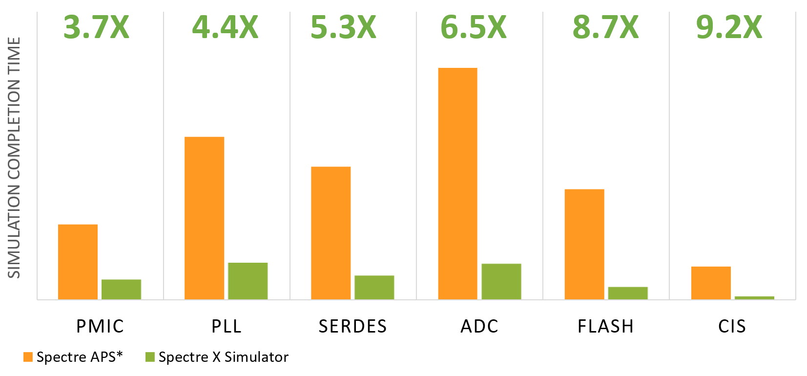
(Image courtesy Cadence)
(Editor update: This article was updated with a more detailed Agile Analog deliverables list based on information received after original publication.)
More info:
Sourcing credit:
- Tim Ramsdale, CEO, Agile Analog
- Steven Lewis, Product Management Director, Custom IC and PCB Group, Cadence
- Hany Elhak, Product Management Director, Simulation and Characterization, Custon IC and PCB Group, Cadence


What do you think of Agile Analog’s and Cadence’s new analog releases?