

Synopsys and Imec recently announced that they’d be collaborating on TCAD activities for the 5nm node.
Yup. 5nm. You can count ‘em on one hand.
We get to see lots of ideas on how things might happen in the future, but once you start defining a specific node, well, it’s time to get specific about what that node’s gonna look like. So I had a quick conversation with Imec’s Aaron Thean on what the notable changes would be at that node.
Because, unlike the old days, when each new node made things smaller, perhaps adding a new technique or tweak here and there to help with the shrinkage, these days it seems that, every couple nodes, something big has to change.
Like going from planar transistors to FinFETs. Or introducing double-patterning. And for all that work, it only buys you a couple nodes – you don’t get to reap the reward for the next 20 years. No time to relax; once you’ve gotten the latest major change completed, time to plan the next one.
While, presumably, each node has its share of evolutionary refinements from the prior node, I wanted to zero in on the big changes. One potentially big change that perhaps isn’t so big after all is EUV, but at 5nm, they’ll still need double-patterning – even with EUV. So hopefully EUV won’t be new at that point – what a drag to have a new litho technology that can free us from double-patterning, only to have it delayed to the point where it also needs double-patterning. Doh!
So that’s not the big one. I hope. The big change is likely to be transistor orientation – again. He sees FinFETs living on down through the 7nm node, but below that, routing challenges are finally going to be too great. At 7 nm, the channel will likely be nanowires instead of a fin, but it will still be horizontal. At the 5nm node, they’re looking at flipping that nanowire up to make it vertical.
In other words, they’ll grow a “forest” of these – well, what I call “pins” – and create transistors out of them. I’ve referred to these in the past as “pinFETs.” Imec refers to them as “VFETs.”
By standing the channel up, you obviously reduce the transistor footprint dramatically. This frees up more routing room. But there’s also another big change: rather than the channel being contacted on the left and right, it’s now contacted on the top and bottom. That messes up the old convenient front-end and back-end distinction. Instead of all the interconnect going on top of the transistors, now the channel will reside between two layers of interconnect. So some of the interconnect will go down before the transistor is built.
They’ve done some trial layouts and have found a rather significant reduction in area by using such a transistor, as exemplified by the NAND gate below.
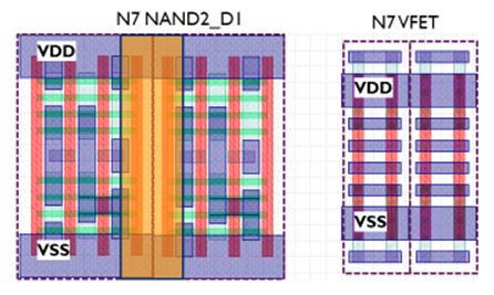
Image courtesy Imec
And when will all of this be coming to a fab near you? He sees 7nm risk starts in the 2018 timeframe; 5nm will lag that by only a couple years: 2020.
Oh, and in case you’re reserving time in your calendar, 3-4nm risk starts are anticipated in the 2022-24 range.
I can hardly wait.


