

We’ve been talking about through-silicon vias (TSVs) for years now, but 2.5D and 3D ICs are still trickling out at the high end.
Processing costs aside, one contributor to higher cost is the impact of TSVs on die size. While we debate the best ways to save a nanometer or two here and there, TSVs operate on a scale three orders of magnitude bigger: microns. And a good part of the reason is aspect ratio: at the current limit of 10:1 or so, then, if you want a 150-µm deep hole, you’re going to need to make it 15 µm wide. If we could improve the aspect ratio, then we could narrow down those TSVs and release some silicon area.
One of the main limiters to the aspect ratio is the ability to fill them cleanly with metal. In order to ensure that there aren’t voids along any of the surfaces, a seed layer is needed. And that seed layer has to be deposited in a well-controlled, uniform manner.
For the metals used as the seed, physical vapor deposition (PDV) – where vaporized material condenses on surfaces in a vacuum – tends to work best. But PVD also is most effective when coating a horizontal surface. Seeding a TSV is most decidedly not horizontal. You need to cover the sides and the bottom at equal rates.
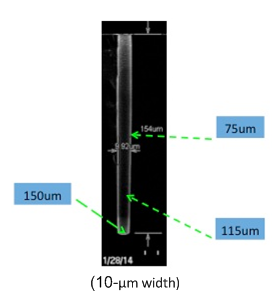 That challenge notwithstanding, Tango Systems announced a couple of months ago that they have now moved the aspect-ratio bar to 15:1, using PVD. They did this through a combination of control over plasma density and vacuum as well as having magnetons that oscillate under the target. So that 15-µm-wide hole we needed to get 150 µm deep? Now it needs to be only 10 µm wide. (Why bother saving 10 nm when you can save 5000?)
Having bumped the limit by 50%, Tango thinks that this 15:1 bar will last for a while. Yes, achieving deeper might have some benefit, but at the same time as this is happening, wafers are also being thinned more, which reduces the needed depth.
TSVs are but the first application they envision for this new technology. They say that it can also have benefit for MEMS (there’s some long-term news pending there), improving the deposition of backside metals, and – their next target – providing EMI shielding.
You can find more in their announcement.


