“3D XPoint is nothing short of a miracle.” – Alber Ilkbahar
Intel just celebrated the start of its 50th year. For those who were not following closely in 1968, Robert Noyce and Gordon Moore founded Intel Corporation on July 18 of that year. That’s a year after the Summer of Love and three years and change before the introduction of the first commercially successful microprocessor, Intel’s 4004. So the company was not founded to make microprocessors (and certainly not love). The invention, commercialization, and immense success of the microprocessor was a happy accident.
Nope, Intel was founded to design and make memory chips because the step-and-repeat nature of a memory array’s design was the fastest, easiest way to fully exploit the potential of Moore’s Law, named for one of the company’s founders. Semiconductor memory also had a vast potential market. It aimed to replace the highly vulnerable magnetic core memories widely used for mainframe computers and minicomputers. These hand-made core memories were expensive, and attempts to automate their production met with limited success. They were also slow. Semiconductor memories would be cheap and fast by comparison. By 1974, semiconductor memory had won, and magnetic core memory was dying quickly.
Semiconductor memory chip sales (largely DRAMs) represented the bulk of Intel’s revenue until 1981. In fact, after inventing the microprocessor in 1971, Intel started to drop behind a growing number of microprocessor competitors including Motorola Semiconductor and Zilog. Then IBM introduced the IBM 5150 (aka the IBM PC) based on Intel’s 8088 microprocessor, and Intel’s world tilted. The company became the new Intel, driven by the very microprocessor it had introduced to the world. Intel management, led by Andy Grove, decided to abandon the DRAM business at the end of 1984. Then, based largely on microprocessor sales, Intel grew to become the world’s largest semiconductor vendor in 1992.
According to Gartner, Intel kept its top spot on that list from 1992 until the beginning of 2018 when Samsung’s astonishing 52.6% year-over-year sales growth in 2017 pushed it into first position. (Most of that growth was in semiconductor memory and was due to higher prices.)
How very embarrassing for Intel.
On August 8, Intel held a day-long “Data-Centric Innovation Summit” in an auditorium on its Santa Clara HQ campus. Although the summit was not billed as a response to the company’s drop from its number-one status in the semiconductor pecking order, the topics discussed certainly addressed what Intel intends to do about revenue growth in the immediate future. Essentially, the company’s coming out fighting. The business details from the summit are informative, especially because they flavor the way Intel is now presenting its technology and product portfolios.
The morning started with Intel’s EVP and GM of the Data Center Group Navin Shenoy projecting a simple slide, shown in Figure 1, to make sure all of us in the audience (media, investors, and analysts) understood that the future is data.

Figure 1: Intel’s Navin Shenoy says that data defines the future, including Intel’s future. (Image source: Intel)
“Data defines the future of the industry and of Intel,” said Shenoy, who then said that half of Intel’s annual sales revenue is already “data-centric.” Getting more specific, Shenoy explained that 90% of all the data ever generated was created in the last two years and that only 1% of that data was used for business value. This leaves whole industries ripe for disruption, starting with transportation.
“The car is the greatest data collector in the world,” and each car on the road is capable of generating 4Tbytes of data per hour, explained Shenoy. The data comes largely from the cameras and other imaging sensors on the vehicle. Imagine real-time mapping and data collection on an unprecedented scale.
This amount of data coming from all those operating vehicles cannot be simply sent to the cloud. Some must be processed locally. Some must be sent to the cloud. Some must be discarded. There’s a lot of processing, networking, and storage involved in the car and in the cloud, with plenty of communications between the two. Intel plans to sell its chips into applications just like this. Shenoy’s mantra of the day was “move data faster, store more data, process everything.”
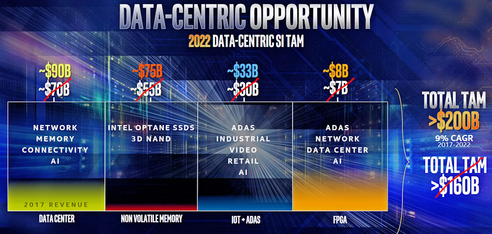
It’s at this point that Shenoy’s presentation directly addressed Intel’s relative lack of growth versus Samsung. He focused on TAMs (total available markets as measured in dollars). Figure 2 shows Shenoy’s version of Intel’s new, data-centric happy hunting ground:

Figure 2: Intel’s Data-Centric TAMs (Image source: Intel)
The top of Figure 2 lists the TAMs, which total $206 billion in 2022. Of that, the “tiny” $8 billion FPGA TAM (the FPGA label appears in small print along the bottom of Figure 2) jumps the total TAM across the $200 billion line.
Well, $200 billion is a big number in anyone’s book. Intel thinks it has perhaps 20% of these markets today, so there’s plenty of headroom for company growth. That was the day’s message for investors and financial analysts.
But EEJournal isn’t a financial publication; it’s a technical publication, so let’s now discuss the semiconductor technology that surfaced during Intel’s 2018 Data-Centric Innovation Summit. Intel expects these technologies to help carry the company to its revenue goals. There was a lot of technology to discuss, and much of it was not processor-centric. I’ll discuss two of these technologies in this article.
Fast Ethernet and Smart NICs
Surprisingly, the first technology I want to discuss was the announcement of Intel’s new Cascade Glacier Smart NIC, which is a “high-speed” Ethernet PCIe card based on Intel’s (formerly Altera’s) Arria 10 FPGAs. Intel is currently sampling the Cascade Glacier Smart NIC (network interface card) to selected customers and plans to make the card generally available in the first quarter of 2019. Smart NICs aren’t new to the industry, just to Intel. They move processing away from server processors and into the NIC. This frees the processor to do more application processing by moving network-related processing such as packet processing onto the Smart NIC.
In the previous paragraph, I’ve put “high-speed” in quote marks because Intel’s Cascade Glacier Smart NIC is currently equipped with two 25Gbps Ethernet ports. If you’re coming from Intel’s traditional networking world of 10/100/1000Mbps and 10Gbps “foundational” Ethernet NICs, then 25Gbps is indeed fast. But the world of FPGA-accelerated Ethernet Smart NICs isn’t new with Intel’s Cascade Glacier. In the current world of Smart NICs, sporting two 25Gbps Ethernet ports makes you a plugger. For example, Netcope’s NFB-200G2QL Smart NIC incorporates a pair of 100Gbps Ethernet ports while Bittware’s XUPP3R PCIe card has four such ports. (Well, technically they’re all QSFP optical cages for active 100Gbps fiber-optic cables.) Both of these boards are based on Xilinx Virtex UltraScale+ FPGAs.
To be fair, Intel announced plans to boost the Ethernet speeds of the Cascade Glacier Smart NIC to 100GbE (Gigabit Ethernet) “in the future” but the future’s already here for other PCIe Smart NIC vendors.
That’s not to say Intel shouldn’t do well in the Smart NIC market. With its 98% share of server processors in the world’s data centers, its intense focus on systems engineering and software for the data center, and its immense engineering resources, Intel has a big, inherent advantage for nearly any kind of product it wants to introduce into this market.
Optane Disrupts the Memory Hierarchy
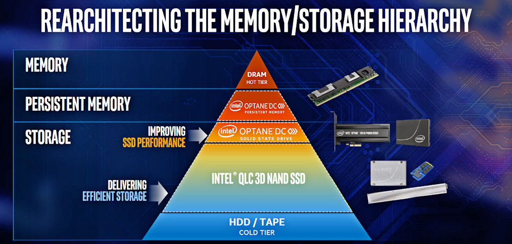
The second technology that was heavily discussed at Intel’s Data-Centric Innovation Summit is the Optane non-volatile memory, which is based on 3D XPoint memory technology that Intel jointly developed with Micron. On July 16, Intel and Micron announced that they were parting ways on this joint venture after 12 years of development. However, that announcement in no way signals the end of the technology. In fact Intel’s rolling it out in two ways, and both disrupt the memory hierarchy, shown in Figure 3, as Intel’s VP and GM of Memory & Storage Solutions Alper Ilkbahar explained. (Real memory hierarchy aficionados will note that processor registers and several layers of cache memory are missing from this diagram’s apex. I guess the slide makers at Intel just couldn’t fit them on the slide, but they’re there inside of the processor nevertheless.)

Figure 3: The Memory Hierarchy with Optane added. (Image source: Intel)
Optane’s first form is called Optane DC Persistent Memory. In this form, Optane non-volatile memory is packaged in a pin-compatible DDR4 DIMM and can be plugged into the DIMM slots of Intel Skylake motherboards just like DRAM DIMMs. However, pin-compatibility does not carry over to timing compatibility. The Optane DC Persistent Memory DIMMs require a different memory controller with different signal timing and sequencing, so Intel has appropriately reworked the memory controllers in its 14nm Cascade Lake Xeon processor, which the company plans to roll out later in 2018. (Note that Intel is also packaging its Optane memory into SSDs, which are faster than NAND-based SSDs and fit into the storage portion of the memory hierarchy shown in Figure 3.)
On the memory hierarchy chart, Optane DC Persistent Memory slots in just behind DRAM, which is not about to be obsoleted. To me, this positioning implies that the Optane DIMMs are somewhat slower than DRAMs, but they compensate with two important characteristics: they’re denser, and they’re non-volatile. Because they’re denser—Intel’s offering 512Gbyte Optane DC DIMMs—you can fit a lot more memory on a server motherboard using the same number of DIMM slots.
That extra memory is located directly in the processor’s memory space, so load and store machine instructions directly access those Optane memory locations with a latency on the order of 100nsec. Compare that to the fastest access latencies of the current SSDs based on non-volatile memory, which need on the order of 100 microseconds or more to go through the appropriate read and write API calls to a file system. Persistent databases stored in Optane memory run 1000x faster.
To emphasize this fact, Ilkbahar started a demo at the beginning of his talk. The demo ran on a standard server without Optane DC Persistent Memory. The demo’s objective was simply to bring up a server after a shutdown, as might be done after maintenance or an upgrade, and then load a database from the server’s SSD. After 17 minutes, the demo had gone about half way. The whole demo required 35 minutes or so—which was more time than Ilkbahar had for his talk. Ilkbahar then started the same demo running on a server with Optane DC Persistent Memory. Because the database was stored in non-volatile Optane memory in the server processor’s memory address space, it was already resident when the server booted and didn’t need to be reloaded. That demo took 16 seconds. The 35-minute difference in boot time translates into real revenue for data centers.
“3D XPoint is nothing short of a miracle,” said Ilkbahar.
Earlier that day, Navin Shenoy had announced that Intel’s Optane DC Persistent Memory was now in production and that the first production DIMM had shipped the previous day. (It’s not clear that Intel shipped more than one that day. You know how these things go with announcements like this.) He then called up on stage Google Cloud’s VP of Platforms Bart Sano and handed one of the production Optane DC Persistent Memory DIMMs to him. Sano joked that he couldn’t wait to get back to Google to torture the memory.
Taking full advantage of a new layer in the memory hierarchy will not happen automatically. It never has. Firmware, BIOS ROMs, and APIs will need to be rethought and reworked to make full use of this new memory layer in a manner similar to the changes caused by the adoption of one-, two-, and three-level cache memories. Think of it as a full-employment program for a certain class of computer software architects.
Intel’s introduction of these Optane-based products on its 50th anniversary is clearly coming full circle because, after all, the company was originally founded to disrupt the mainframe and minicomputer memory hierarchy—which was based on magnetic cores at the time. And time will tell whether Intel manages to perform the same trick once more, half a century later.


