


Part 1 of this article discussed the Fairchild resistor-transistor logic (RTL) NOR gate ICs used in the Apollo Guidance Computer (AGC) for NASA’s manned lunar program in the 1960s. Ultimately, NASA ordered one million ICs – so many that Fairchild alone was not able to fulfill the orders, so NASA ordered parts from Motorola Semiconductor, Philco, Texas Instruments, Transitron, and Westinghouse. The AGC Block I computers used Fairchild’s original Type G 3-input NOR gate. The AGC’s design required 4100 of these NOR gates. By the time the AGC Block II computer was designed, Fairchild had upped its game and was able to fit two 3-input RTL NOR gates into one 10-pin package, which cut the number of ICs needed in half and allowed Eldon Hall, the designer of the AGC, to fit more capabilities into the Block II design. This dual NOR gate was the Fairchild μL 9915, formerly known as the μL 915 before Fairchild decided that it needed 4-digit part numbers for its ICs.
I thought it might be interesting to see if I could purchase a Fairchild 9915 and try it out. With a little Googling, I found that a parts distributor named MarVac Electronics – located in Costa Mesa, California – had two Sylvania ECG9915 Dual NOR Gate ICs in stock. I ordered them immediately, for $6.49 per IC. The company has no more ECG9915 ICs in stock but still has three ECG9914 dual 2-input NOR gates as of this writing. They’ll cost you $9.99 each, plus shipping. Incidentally, I noticed that MarVac has hundreds of old ECG ICs in stock.
MarVac is one of those dwindling number of mom-and-pop electronics stores that flourished in the latter part of the 20th century and is exactly the kind of place that gray-haired engineers like me like to haunt. The store first opened in 1965. Founder Deno Vaccher, decided to start his own electronics business after working for his brother, Leo, at Orvac Electronics in Fullerton, California. Vaccher wanted to be near the beach, so he opened Marvac in Costa Mesa, just up the street from Newport Beach. He named Marvac for his wife, Marlene Vaccher.
The ECG9915 ICs that MarVac sent to me might have been in stock there since the 1980s. Printing on the adhesive price tags stuck on the plastic bags holding the ICs had faded to invisibility and the polyethylene bags themselves had become fragile with age. The bags shredded at my touch. I didn’t know polyethylene could age like that.
The Sylvania ECG product line was a comprehensive line of replacement parts for all sorts of electronic components, including tubes, transistors, ICs, and IC sockets. Philips purchased Sylvania in 1981 and took over the ECG product line. MarVac shipped me the two ECG9915 ICs in short order. When they arrived, I noticed that the polyethylene bags holding the ICs were marked “PhilipsECG,” which means the ICs inside were bagged after 1981. However, the ICs inside of the bags were marked “SYL” for Sylvania and had a date code of 7419 stamped on the can. So, these ICs were bagged seven or more years after they were manufactured.
Sylvania was not one of the companies that NASA contracted with for 9915 NOR gates, so I was curious about the maker of the semiconductor die in the Sylvania IC. I asked Ken Shirriff about the 9915. Ken is the most accomplished silicon archaeologist I know and is a member of the merry band of technologists that have restored a Block II AGC to working condition, as documented through multiple episodes on Marc Verdiell’s YouTube channel, CuriousMarc.
Ken has delidded and reverse engineered dozens of ICs over the years in his blog, and he’d commented on the layout of the 914, a dual 2-input RTL NOR gate that’s a close cousin of the 9915. However, he’d not cracked open the lid on a 9915, so I sent him one of my two ICs so that he could decapitate it and shoot a die photo. Ken’s photo appears below.

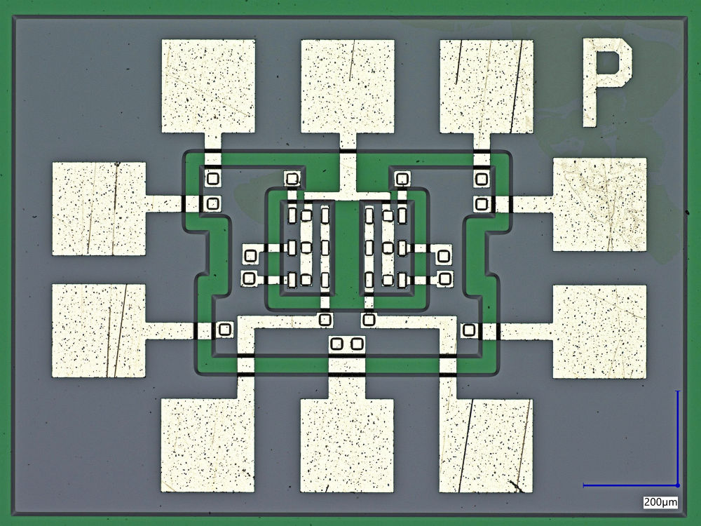
Die photo of a Philips ECG9915 dual 3-input NOR gate. Note the designation “9915 W.” I believe the “W” stands for Westinghouse. Image credit: Ken Shirriff
I was expecting the die in my ECG9915 IC to have been made by Philco, because Philco made the bulk of the 9915 ICs bought by NASA for the AGC program and because GTE Sylvania bought Philco in 1974, the year that these ICs were made. However, a Philco die would have a “P” on it and this die has a “W,” so I’m guessing that Westinghouse was the maker of the chip used in this 9915 IC.
Ken noted that there were a few unused components on the die, so it might have been a multi-purpose die, used to make other types of RTL ICs with various metallization layers. Ken also noted that this layout appeared to be more advanced than the chips used in the AGC.
All that remained was to power up the one remaining 9915 IC that I had and see if it worked after all these years. I was not especially hopeful. Even the polyethylene bags containing the ICs had aged.
Before I could power up the IC, I needed to build a test fixture for the chip because I didn’t want to apply heat and solder to the device’s leads. Although NASA used flat-pack ICs for the AGC Block II computer, the 9915 ICs I’d purchased from MarVac were in 10-pin TO-97 packages, which was more typical for commercial ICs of the early 1960s. I went looking for a TO-97 test socket and found a package of four 10-pin Cinch TO-97 test sockets on eBay. I ordered the sockets. When they arrived, I discovered that only one of the sockets was a 10-pin TO-97 socket. The other three sockets were 8-pin TO-99 sockets. At least I ended up with one socket for a test fixture. I may have overbuilt the test fixture, as you can see in the image below. It incorporates about $20 worth of parts to test a $6.49 IC.

Test fixture for the 9915 dual 3-input NOR gate. If you look closely, you can see “SYL” marked on the IC’s can. Image credit: Steve Leibson
I exercised some caution when powering up the 9915 IC in the test fixture. I slowly brought the supply voltage up to 3.5 volts. Static tests with a DMM and a pullup resistor showed that both 3-input NOR gates in the package worked. NASA’s AGC ran on a four-phase 1.024MHz clock, divided down from a 2.048MHz crystal oscillator, so I started slowly with a square wave at around 300 Hz. Soon, I’d “cranked it up to 11” and applied a 5MHz square wave. The result was a 5MHz output from one of the NOR gates with about a 20nsec delay through the gate for the falling edge of the output and somewhat longer for the rising edge. My HP 6236B power supply and Wavetek Model 184 waveform generator are both period-correct from the 1970s, but my Siglent 1202X-E digital scope is strictly a 21st-century instrument. The resulting waveform appears below.
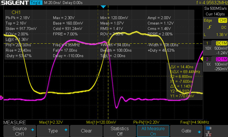
A 5MHz square wave applied to the 9915 NOR gate (yellow trace) results in an inverted output with about a 20nsec delay (purple trace). Image credit: Steve Leibson
You can see from the purple waveform, which shows the NOR gate’s output, that the fall time is much faster than the rise time. That’s because the RTL gate uses a transistor to actively drive the output low, but it has only a 640-ohm resistor to pull the output high.
The 9915’s published propagation delay numbers are 32 and 20 nsec respectively for the rising and falling edges of the output. Those are the only latency numbers on the data sheet. Apparently, Fairchild had not developed a minimum/maximum/typical approach to rating the delays in their ICs by the time the 9915 appeared, which became standard fare on data sheets published in the era of TTL ICs.
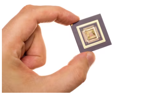
By an interesting coincidence, a team led by Professor Santosh Kurinec at the Rochester Institute of Technology (RIT) is currently recreating the 9915 IC using the Philco chip layout, which looks much cleaner than the layout on the die in the 9915s I’d ordered from MarVac. Professor Kurinec advises undergraduate and graduate students in RIT’s Microelectronic Engineering program, which includes cleanroom work. Pamela Hall, daughter of AGC designer Eldon Hall, provided Professor Kurinec with one of the original ICs used in the AGC program. This particular IC was made by Philco, based on the die layout, which the team at RIT recreated with modern EDA tools.
Die photo from the Rochester Institute of Technology (RIT) project to recreate the Fairchild 9915 dual 3-input NOR gate. This design replicates the Philco layout and appears to be much cleaner than the die in the ECG9915 ICs I purchased. Image credit: Professor Santosh Kurinec, RIT
The Fairchild Type G 3-input RTL NOR gate, later renamed the μL 903, was one of the three original ICs in Fairchild’s first logic IC family. It became the foundational component for the NASA AGC and several thousand of Fairchild’s 9915 dual 3-input RTL NOR gate became the first logic ICs to land on the moon, along with the Apollo astronauts. Without the 9915, Apollo might not have reached the moon. Without the Apollo AGC, Fairchild’s RTL logic family might not have become the breakout semiconductor product of the early 1960s. Each needed the other for success.
References
Apollo Guidance Computer Part 1: Restoring the computer that put man on the Moon, CuriousMarc, YouTube, 2019
Lenore Edman, Uncovering the Silicon: μL914, Evil Mad Scientist, May 16, 2019
Eldon C. Hall, “Journey to the Moon: The History of the Apollo Guidance Computer,” American Institute of Aeronautics and Astronautics, 1996


Always happy to see you untangling the threads of history. Unfortunately, the link to Lenore’s article is a 404 since the Evil Mad folks decamped to the East Coast. Can you provide an updated link?
Thanks!
Hi Jack. Thanks for alerting me to the broken link. I’ve just fixed and verified it in the article.