There’s a memory access technology out there that makes some pretty bold promises. If you take only the top-level messaging away, it sounds like, well, magic. And if you think through it a bit more, you start to squint your eyes and go, “Hmmmm… How is that even possible?”
The technology is called “scatter/gather,” and my goal was to ferret out exactly what this means and what you should expect when using it – and, in particular, understanding the promise of “single-cycle access.”
We’ll start with a quick review of the concept, sharpen which kind of scatter/gather we’re talking about, and then bore into why it’s useful and how it can ultimately work. In case I might have thought I was researching something basic here that was obvious to the rest of the world, it bears noting that there’s some mystery in how this all works – and that’s intentional. Cadence was willing to discuss their technology – to a point; another provider of scatter/gather, CEVA, was not even willing to confirm or deny the most high-level statement about how scatter/gather might work without an NDA, saying that their competitors had already copied too much of their technology.
So, when we get into details, it bears noting that the details will correspond to Cadence’s implementation in particular. That discussion should help to tease out the sorts of things this technology involves, so, even if it doesn’t describe someone else’s approach, at least we know what questions to ask.
Scatter/Gather: the Basic Idea
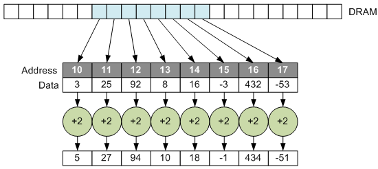
Let’s start with the basic notion of scatter/gather. We’re used to organizing our memories by row. Caches are built from rows – you want one piece of data, you get the whole row. If you want to manage your performance tightly, then you try to have as many related variables as possible on the same row so that you get more bang for your caching buck and reduce your cache misses.
The nice thing about a row of memory is that, especially with vector structures like SIMD (single-instruction, multiple data), you can operate on multiple pieces of data at the same time, in parallel. At the very least, if you can’t do it in parallel, then you can loop along the row for the operation without further fetching hassles.

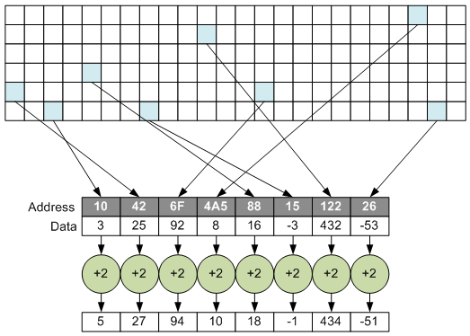
But there are several contexts where the world doesn’t cooperate with this row-by-row structure. What if you want to be able to do is exactly that same thing, but without the requirement that addresses be contiguous?

This isn’t so easy to do, since you need lots of fetches to populate a vector; you can’t just copy over a chunk of memory and get busy operating on it. The idea is to find a way to “gather” data from far-flung locations, work with them as a single vector, and then, if desired, take the results and “scatter” them back out into their original far-flung locations.
Different Scatter/Gather applications
If you Google “scatter/gather,” you will find, as I did, that there are a lot of search returns relating to Windows. Poking through those reveals that there are at least four different contexts for the use of scatter/gather.
- A single block of in-memory data may represent data from a file that has been fractured into various sectors across the storage medium.
- A single in-memory buffer, if too large, may cause problems due to memory fragmentation. It can be more easily managed if it’s stored in smaller fragments, but this requires management to make them “look” contiguous.
- Network traffic streams may be split up as they arrive, with various buckets in memory. This is referred to as “Scatter/gather I/O.” In a way, this is the reverse of other applications. In other applications, scattered data is brought together in the processor. With this streaming version, it’s a unified stream that then gets scattered about as it arrives at the processor.
- Embedded systems may require low-level access to data that’s scattered throughout DRAM, treating it as contiguous. The illustrations above reflect this application. As we’ll see, vision is a major driver of this usage.
The focus for this article is going to be the last one. This gets to the interface between DRAM and processor and tries to overcome the row-oriented nature of DRAM data.
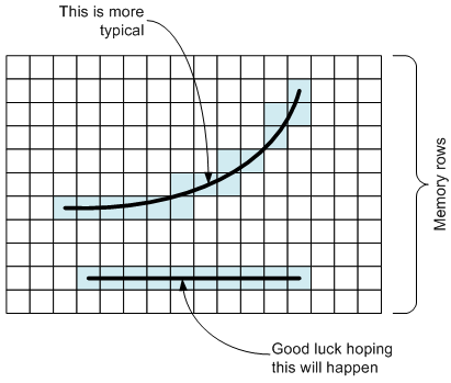
The reason this is popular for vision is that various features in an image will have random orientations with respect to the memory. The algorithms will want to work on the features at a higher level of abstraction, without having to get bogged down (and slowed down, potentially) due to the row-oriented nature of memory.
As an example, let’s assume that a particular edge is of interest. It would be really convenient if that edge happened to lie along a row in memory, but that’s not typically going to be the case. I won’t even muse on how hard it would be to solve this issue by doing multiple rotations of the image to line edges up with rows when needed (and they’re mostly not going to be lines anyway).

If a single operation is to be performed on this edge – say, sharpening, for example – then you’d like to be able to do it in one fell swoop, using the edge as a vector and operating on each pixel independently, in parallel. That’s not easy to do for a randomly oriented edge.
Scatter/gather is put forth as the solution to this issue. But many descriptions of scatter/gather speak broadly in terms of being able to access non-contiguous memory locations in a single clock cycle, or, effectively, in that one fell swoop. Knowing how DRAM works made this, to me at least, a dubious claim. So my goal here was to dig a level deeper to see what expectations you should have of scatter/gather functions, bearing in mind that there is no one definition of how this is supposed to work. Different vendors may have different implementations, and, given my experience so far, this is an area of competitive differentiation.
Scatter/Gather: the Cadence Version
Cadence markets what they call a “SuperGather” capability. Part of my first goal was to figure out whether this was scatter/gather on steroids, or just their brand of scatter/gather. It’s the latter. So that’s all well and good. The next question then is, “How does this work?”
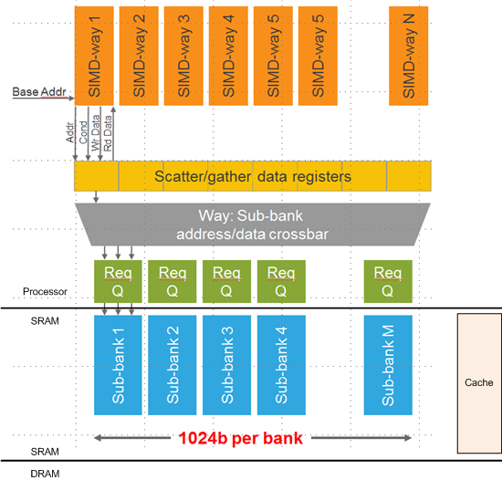
The following diagram illustrates the architecture of the solution. Not shown is the management hardware that handles all the control aspects of this. And, as you’ll see, control can be complicated.

(Based on an image courtesy Cadence)
What’s shown is a “channel,” if you will, for accessing DRAM independently of the normal cache mechanism (which I added just to show that it would exist in parallel with this scatter/gather block).
In the context of an SoC, the DRAM will presumably consist of one or more chips external to the SoC; the SRAM (implementing cache and “sub-banks”) will be embedded into the SoC. In the case of scatter/gather, the SRAM is a so-called tightly coupled memory (TCM), giving the processor quick access.
The blue “sub-banks” are filled from DRAM via DMA. So, in fact, there will be two such SRAM blocks; one will be in use while the other is being filled to reduce the impact of the time required to get the data from DRAM. So, for instance, the entire block that contains the edge shown above might be loaded into the sub-banks. Exactly how many sub-banks are used is determined by each customer.
That brings the memory containing the edge much closer to the processor, but the desired cells are still scattered about within the contiguous memory structure. The next step is handled by the blocks labeled “Req Q,” which stands for “request queue.”
And here’s where we get more subtle. Getting access to a non-contiguous vector takes some work, so the first thing that happens is that you request the data. Each request queue can operate in parallel, so if you have, say, four locations of interest, then, if each resides in a separate sub-bank, you can load those four up in parallel. If, say, two happen to be in the same sub-bank, then those two requests will be fulfilled one after the other.
So, even at this point, we’re not getting to the data in a single access. Even if we give credit for the DMA happening in the background and not taking extra time, accessing multiple locations within a single sub-bank will have to be done one request at a time. So the time it takes for this depends on how the data lays out in the sub-banks.
Of course, I should be more explicit about what “this” means. Each piece of data is going to be required by one of the “ways” in the SIMD structure. Each way operates on a single piece of data, as per traditional SIMD. It’s just the complication of the scattering that’s the problem.
So when data is requested, then, based on the way that needs it and the address in the sub-banks, the control logic will place a request in the queue and, when the data is retrieved, will route it via the crossbar (single clock cycle) into the register location corresponding to the way that needs the data.
The data request, being the first in the two-part operation, may take an unpredictable amount of time. It depends on what other requests are pending ahead of it in the queue as well as how well distributed the requests are throughout the sub-banks. So this instruction is non-blocking. When you know you’re going to need the data, you kick off this process of loading the scatter/gather data registers. At some future point, you issue a second instruction so that you can use the data. This instruction is blocking, so if you issue it too early, before all the requests have been fulfilled, you may end up waiting around for it to finish.
Once that register is full, you can operate on the data in single-cycle operations (or in parallel for more complex multi-cycle operations – all part of the one-fell-swoop thing). This is where the single-cycle access holds true.
Based on the cost of gathering the data, it would make sense to do as much work as possible while it’s in place. If you have five edges that you want to manipulate using three operations, then it would likely be faster to perform all three steps for each edge rather than doing all edges for each step.
The logic controlling this whole beast (not shown on the diagram) would appear to be pretty complicated. It has to track requests in process, perhaps taking some out of order if they happen to fall into free sub-banks. I had a question about reading data into some banks while writing from others; that’s where I hit Cadence’s transparency limit. They weren’t willing to go into that level of detail.
And, speaking of writing back, while I’ve focused on the gather aspect, the scatter operation is pretty much the same thing in reverse, except that only a single instruction is required for that (as opposed to the two-phase gather operation).
There’s lots more detail we could explore, although you’re more likely to get info on those details than I am, since you’re more likely to sign an NDA than I am. (After all, my job is to disclose…) But I feel like my basic question has been answered: No, you’re not getting single-cycle access to multiple non-contiguous DRAM memory locations directly. There’s a fair bit of rummaging around required to do the gathering and scattering. But, done effectively, you can then operate very efficiently on that data register.
More info:
Cadence/Tensilica Vision IP (with scatter/gather)


Do you know of other scatter/gather implementations?
Interesting — thank you for the overview of this scatter-gather technology.
When I started reading this article, I was secretly hoping for a fundamentally different SDRAM architecture. An SDRAM that could implement a configurable stride (instead of contiguous addresses) when opening a row would be fantastic, but I can’t imagine how that could be implemented electrically.
It looks like the main advantage of the technology you describe is that many pending scatter-gather requests can be combined (where they overlap) into a reduced number of prefetches from SDRAM. Even without address overlaps, this technology could be a good alternative to designing one’s own prefetch framework.
When external DRAM RAS/CAS/PreCharge timings are the limiting latency in processing data, depending on scatter/gather rather than optimal data packing/ordering is certainly the best way to guarantee the worst possible memory bandwidth BY DESIGN. I certainly didn’t see anything in the article which suggests otherwise.
Best possible memory bandwidth is obtained with burst Column cycles sharing the same RAS/PreCharge cycle latencies. This performance enhancement is exploited by memory cache designs to significantly improve performance of algorithms that are optimized for locality with optimal cache line data packing.
The processor/ALU/pipeline is almost always running at a higher clock rate than basic RAS/CAS/PreCharge memory latencies, typically by a factor of 10 or more.
Anything that by design, which yields sub-optimal memory performance in comparison to best case burst access, probably isn’t a good idea if performance is important.
Generally one can choose data packing/ordering optimized for processing … and then if needed, reformat for export to storage or some device specified packing/ordering as part of the I/O setup. And in some cases, careful design of the cache size/depth/width/LineLength can completely mask this.
I share the skepticism because it would require a custom hardware design.
“RAS/CAS/PreCharge memory latencies” pertains to memory chips but the real key is the interconnect bus delay, cache/TLB control algorithm, and the time to transfer blocks of data in the multi-level cache hierarchies.
The I/O channels in mainframe systems accessed memory directly, treating the cache as a part of the processor. Of course some cache lines had to be invalidated when new data arrived.
“THE DEVIL IS IN THE DETAILS”, and it is too bad that hype has over shadowed understanding of how hardware actually works.
This is a conceptual algorithm rather than a design.
I apologize for my knee jerk reaction yesterday.
At first it looked like a new memory control for general purpose computing, but it is a DSP IP with a custom DMA memory interface that has several independent memory banks so the classical cache line problem is by-passed.
Another win for heterogeneous where blocks of data are handed off for customized processing.
@Karl — sure multiple banks/channels can offer concurrent read/write, or even multiply sourced reads/write — but each channel still has the native single access or burst fill performance timings.
Now look at the last three figures above, where Cadence is expecting the SoC system designer to provide a multi-channel external cache, to buffer sparse row utilization. In the third figure, notice Byron’s comment “Good Luck hoping this will happen”.
In most cache designs a read miss forces a cache line to be invalidated (possible write back), then does a full width cache line fill using using a common PreCharge/Ras cycle, followed by a burst of Row Cas cycles. This is normally significantly longer latency than a single access PreCharge/Ras/Cas cycle.
Organizing data to be processed as sparse with scatter/gather, where much of the data is not accessed, will significantly limit processing speed due to memory/cache latency bottlenecks. And possibly, actually very likely, will generate significantly slower performance than initially expected (or advertised) by the system designer(s).
Worst case in this sparse scatter/gather approach, is a data layout pattern where ALL accesses end up in the same sub-bank in the last figure, and the other sub-banks contain data never accessed. The cache will thrash significantly with misses/fills, and system performance can become less than 5% of the expected design performance assuming even distribution of data across sub-channels. And less than 1% of a design where data is organized and packed to be cache optimized.
Thus I started my first comment with:
When external DRAM RAS/CAS/PreCharge timings are the limiting latency in processing data, depending on scatter/gather rather than optimal data packing/ordering is certainly the best way to guarantee the worst possible memory bandwidth BY DESIGN. I certainly didn’t see anything in the article which suggests otherwise.
Now you might say that no one would be that stupid as to pack all accessed data into a single subchannel. With the number of sub-channels being 2^n (where n is 1, 2 or 3), it’s also pretty likely that the underlying data structure to be processed will have the same 2^n size (1, 2, 4, or 8 lines), or a multiple of that.
In 40 years of performance consulting I’ve seen FAR worse.
This same VERY common problem where the applications data structure is exactly a cache line width, or multiple, hits designers every day … and they scratch their heads wondering why their system is slow. When the applications memory performance is a single access per cache line, and the cache is thrashing hard, it’s hard to see why if you do not understand the underlying hardware design.
I’ve also seen it where the data structure is a 2^n multiple of cache line size, so that only 1/2 or 1/4 or 1/8th of the cache columns are utilized, and the rest of the cache idle. This is very common with dynamically allocated C++ structures with a power of two heap doing allocations.
Worse yet, is the first several cache columns frequently have 50-80% of the accesses, because of dynamic allocation by page size, and dozens of call contexts in multiple layers of dynamically linked libraries.
When you do not consider the basic hardware design, other apparently good design choices quickly yield sub-optimal results.
If you are the Soc designer for this system, make sure you include extensive cache hit/miss/fault statistics by sub-channel in your cache design. You may never figure out why some application/things are slow otherwise.
What is FAR worse?
An 8-way time division multiplexor to “fairly share” memory between 6 processors and 2 DMA channels — no priority accesses to starve another channel, no contention based allocations, just straight channel 1 gets only time slot 1, channel 2 gets only time slot 2, etc. The basic memory time slot has a latency of PreCharge/Ras/Cas.
In the 1970’s and early 1980’s the largest third party peripheral company (disk, tape, communications, etc) pretty much held the majority of the 3rd party market. In the mid-80’s they wanted to become a computer company and designed a multiprocessor M68K system with such a memory allocation design.
With each processor starved to 1/8th DRAM performance, it was a total dog, slower than a single processor design, and unable to process incoming RS232 data fast enough to avoid dropping a 1200 baud terminals function key burst sequences.
The engineer that made that mistake, was one of the best disk/tape controller designers in the industry. The company owner made the mistake of thinking he was also qualified to be a systems level architect.
The mistake caused the company to fail quickly, without any chance of recovery.
There are worse yet mistakes …. care to share those you have seen?