

A couple of months back, Open Silicon announced an HBM2 IP subsystem. Those of us who don’t deal on a daily basis with – what to call it? High intensity memory? – might be vaguely aware that some standards of some sort exist, but are used by other people. Which means we keep but a vague impression of what it’s all about: stacks of memory or some such craziness.
But there’s more to the story than that, and the announcement was a something of a kick in the butt for me to try to ferret out what was going on with these 3D chunks of memory. Because there’s not just one way of doing it – there are two major approaches, with two different goals. One is High-Bandwidth Memory (HBM) (for you static-sticians out there, no, it’s not “human body model”); the other is the Hybrid Memory Cube (HMC). And, given that the announcement was about HBM2, there would appear to be more than one generation underway. So what’s the deal here?
Both of these “standards” join a variety of other standards that are part of this evolution. I put “standards” in quotes because only the HBM approach has been standardized by an independent body, JEDEC. There’s a “standard” for HMC as well, but it’s from the HMC Consortium – not independent of the technology. This gets to the fuzziness of the word “standard” that we looked at recently.
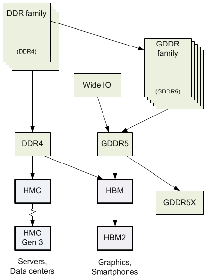
That said, they join DDR – the basic DRAM interface – on its 4th generation; GDDR – a DDR variant dedicated to memory for graphics – on its 5th generation; and the Wide-IO standard, which establishes an interface between memories that would be impractical if done by wires, but can work wonders with a stack of memory chips using microbumps and through-silicon vias (TSVs).
Strictly from a point of view of trying to understand the family relationships between these, I’ve sketched something of a family tree below based on my interwebs ferreting. Specifically, the HBM side of things is targeted largely at improving graphics processing, while HMC is intended more for servers in data centers, to oversimplify.
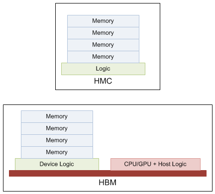
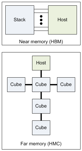
Let’s start with a big high-level difference. As a graphics-oriented standard, HBM has an architecture that can include a processor (often a GPU) in the same package, providing a tightly-coupled high-speed processing unit. HMC devices, on the other hand, are intended to be connected up to a processor (or “host”) with the ability to “chain” multiple memories for higher capacity. More on those bits in a moment.
Both have an architectural notion that separates the logic of a controller and the actual bit cells themselves. Putting the logic on a separate chip places it on a standard CMOS process, without all the special memory stuff. But HBM further splits that logic into “device” logic and “host” logic, with the difference largely being the level of abstraction. Host logic interprets commands sent by a processor; device logic largely does the work that DDR logic performs – except that it’s no longer on the same die as the memory.
Part of the logic to this is that the memory stack itself will be made by a memory company; the combination with a GPU or CPU might be done by a different company. So this separates out the logic that is more intimate with the memory from the higher-level logic that drives the memory.
Since the original publication, there’s been some confusion that I should clear up, and it depends on your view of what constitutes HBM, mostly, but also with HMC.
Let’s do the HMC one: in my research, I saw both 2.5D and 3D versions. It may well be that the 2.5D versions were early, which is why I noted that the preferred – and pretty much only – version you’re going to see today is 3D. However, it’s important to remember that I’m speaking from the standpoint of someone buying the unit. Other than the specific size, as a purchaser, you wouldn’t know (or care) what the internal arrangement of the dice was. In either case, you would simply affix it to your PC board to connect it to your host processor. To avoid further confusion on this score, I’ve eliminated the 2.5D version from the drawing above (which appeared in the original version).
HBM is a bit more subtle, and the confusion comes from the distinction between the pure memory stack and the full memory+processor assembly. The memory stack, as illustrated, is always 3D, including the device logic under that stack. The question is, would you buy just that memory stack? Here’s where the nuance comes.
If you’re buying from, say, AMD, you can get a complete processor+memory unit. It will have a 2.5D internal structure consisting of a 3D stack and a processor on an interposer. As a user, you would simply solder that to your PC board just as you would with HMC (except that, here, you’re not connecting memory to a host – the host is already in the package). As with HMC, you don’t necessarily need to know the internal structure (but I assume that curious people would like to know).
There are other applications –and Open Silicon’s Swamy Irrinki illustrates networking applications as an example – where there is nothing analogous to the off-the-shelf processor, and no complete memory+processor unit is available. Instead, you design and have built an ASIC or SoC for use where the processor is shown above. The memory stacks (3D) are acquired from memory makers, and you create a silicon interposer to co-package the overall assembly as a system-in-package – this is 2.5D. You can do this yourself or through a company like Open Silicon.
The Open Silicon IP solution doesn’t include a host – just the host logic for integration into an ASIC or SoC. But if they do the ASIC/SoC integration for you, then, in fact, they can ship you completed units.
So an overall module with HBM will be 2.5D, whether purchased off the shelf or done custom, even though the memory stack itself is 3D.
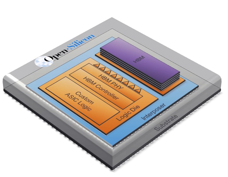
(Image courtesy Open Silicon)
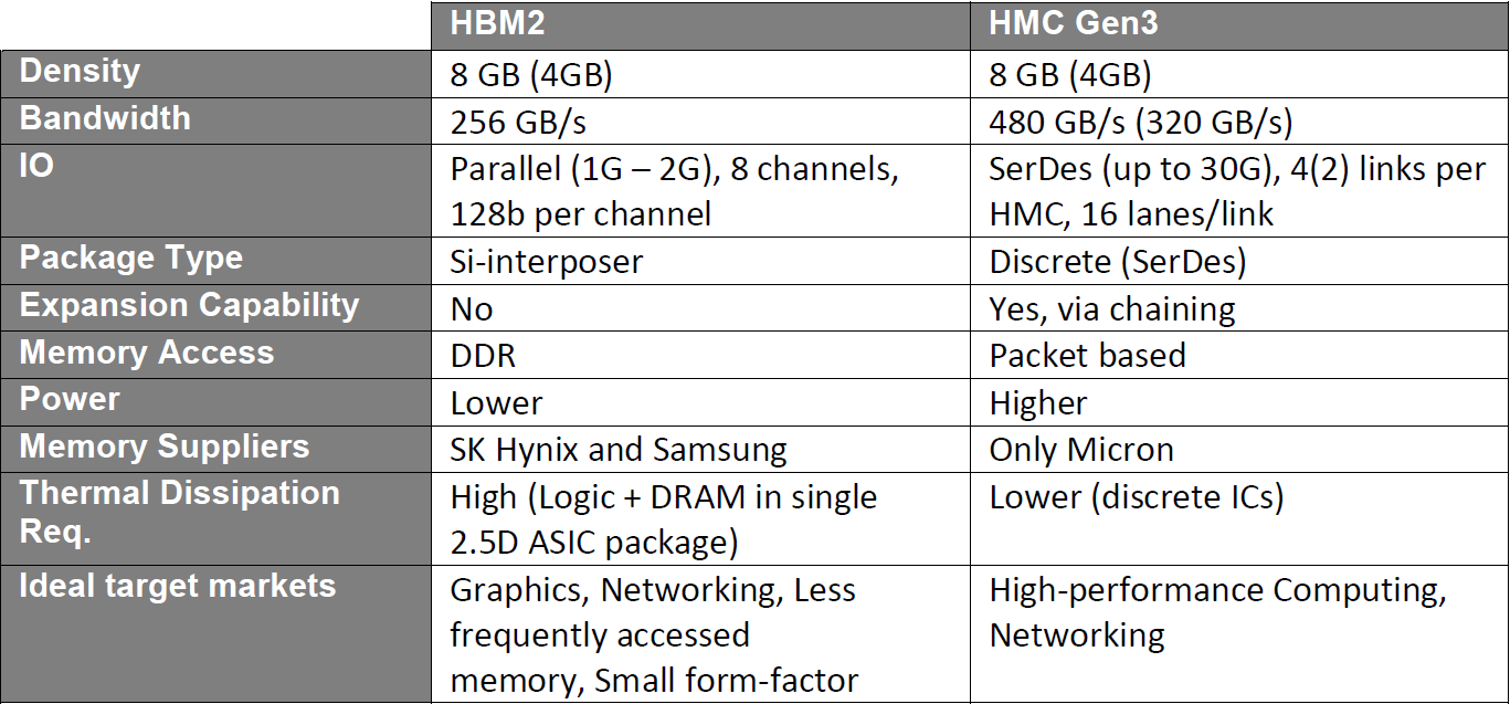
Another difference reflects the backers and suppliers: HMC has pretty much only Micron as a supplier these days (apparently, HP and Microsoft were originally part of the deal, but they’ve backed out). HBM is a Hynix/AMD/Nvidia thing, with primary suppliers SK Hynix and Samsung.
Then there’s the distinction between interfaces. HBM becomes a complete, self-sufficient unit, with memory tightly connected inside the package. This is referred to as “near memory.” It’s not intended that you combine these to get more memory.
HMC, on the other hand, supports the notion of “far memory” – chains of memory that are effectively networked together for attachment to the CPU for a maximum of 8 cubes. Instead of the DDR-based interface that the HBM stack uses, HMC has a packet-based interface that operates over some number of links (2, 4, or 8), each of which has 8 or 16 serdes lanes, each of which can have bandwidth from 10 to 30 Gbps. The largest, fastest devices boast 480 GBps, although, after accounting for overhead, this is more like 320 GBps of actual payload data.
What’s refreshing here is that, unlike so many of the IoT “standards” that compete with each other, these two don’t. There’s no reason why the success of one has to come at the expense of the other. They have different sweet spots, so, as long as both sweet spots survive, both configurations can survive.
Open Silicon has no specific horse in this race, or, perhaps better said, they have both horses in the race. The announcement was about their HBM2 subsystem, but they also have IP for HMC memory as well, providing both ASIC and FPGA versions of the HMC controller.
They’ve put together a handy chart summarizing the differences between HMC (Gen3) and HBM2, reproduced below. Yeah, we didn’t get into the differences between generations; in general, they add speed or variations on links and lanes and such. And there are a number of parameters that we haven’t covered as part of this exceedingly brief overview; further delving is left as an exercise for the reader.
(Source: Open Silicon)
More info:
HBM Specification (requires registration)
HMC Specification (download form)
Open Silicon:
[Edited to clear up confusion regarding 2.5D or 3D configurations]


Which of the 3D memory stacks applies or appeals more to you?
There’s a dimensional problem with memory – a 2D surface with contacts on the edge or a 3D volume with contacts on the surface gets harder to get data in and out of as the density of the memory increases – so an architecture that separates data from compute is fundamentally limited in how well it can perform.
I.e. neither works in the long term, only a PiM (processor in memory) approach avoids that problem.
Intel’s approach of placing the memory a long way from the CPU (probably because of the big heatsinks) means most of the advantage of die-stacking and intrinsic low latency are lost –
https://www.computerworld.com/article/3154051/data-storage/intel-unveils-its-optane-hyperfast-memory.html
– suddenly you only have as many wires as a PCIe slot, and PCB wires don’t go that fast, not to mention all the layers of caching and coherency hardware.