

There’s going to be a new kid in town when we get to 5 nm. Her initials are DSA. And she’s not going to be completely transparent to designers, although tools will likely help to minimize the impact.
We’re talking about directed self-assembly (the D, S, and A in DSA). Which we’ve talked about before – it’s been one of our reliable post-SPIE-Advanced-Litho-conference update topics (whether fundamentals, EDA impact, the impact on how masks relate to actual patterns, or just the latest). And it will be an option, as I suggested, at the 5-nm node (with ongoing 7-nm work to bring it up).
At this year’s SPIE Advanced Litho, Imec’s Roel Gronheit made an update presentation and alluded to the notion of “DSA-friendly design.” That caught my attention, and, in a quick conversation afterwards, he directed me to Mentor Graphics’ Andres Torres, who has been heavily involved in much of the leading DSA work. So I was able to sit down with Andres later and discuss just what it means for a design to be DSA-friendly.
Let’s first review DSA for anyone feeling left out. And I’ve thought of a new analogy to describe what happens. Imagine, oh, let’s say 8-year-old boys and girls. At that age, boys like to hang out with boys and girls with girls. If you put a bunch of them together in a big room, at some point they will self-segregate into two groups: the boys and the girls.
Now let’s imagine that they have to go to – Yuck! – dance class to learn how to be classy young adults. So they get paired up, and here’s where the outrage starts: they have to hold hands. So they do, but they try to stay as far apart as possible without breaking the hand-hold. And the boy of one pair aligns himself to the boy of another pair (better a girl on only one side than on both sides!). And the girls are fine with that, since they also end up with a boy on only one side.
This causes some self-assembly as this sorts out, although it will be pretty random unless you line them up against a wall, forcing them to take on a straight-line configuration.
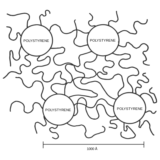
Well, that’s DSA in a nutshell. Two polymers that don’t like to intermix are bound together (making them copolymers) – which they reluctantly accept, but then tolerate by trying to stay as far apart as possible. Using lithography to define guiding patterns (either by physical boundary, like a wall, or by underlying chemical affinity), you can, within limits, coax the copolymers to conform to some kind of pattern. Etching one of the copolymers away then leaves a pattern that can be transferred down into the silicon.
But – and this is important for design and layout – this assembly takes on a periodic character. Boy holds hand with girl, who stands next to another girl that holds hand with boy, who stands next to another boy – and repeat periodically. The length of the period is determined by how long the arms of the boys and girls are.
Yeah, in real life, kids don’t all have the same arm length, but in the chemical equivalent, it’s the length of the polymer that sets up the period. And that length presumably has less variation than the lengths of 8-year-olds’ arms.
OK, so that’s a general description, but at this point we’ll depart from the analogy because it starts to fail. There are several different “shapes” that can be created using DSA, depending on the polymers. This has to do with how they self-assemble (which is largely a thermodynamic process of finding a low-energy state).
The two most important configurations are cylindrical and so-called lamellar. The latter is essentially a vertical line, taller than it is wide. For any of you geologists, you might think of it as being similar to a dike (not in the canal sense). Architects might picture it as a very long pony wall. Cylinders are useful for contact and via holes; lamellae are useful for fins in FinFETs.
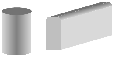
With cylinders, you can create smaller vias, closer together, with smoother edges than is possible with direct lithography, and you can reduce your mask count by at least 1. There appears to be active interest in this. The fins, on the other hand, don’t provide a clear cost advantage versus SADP (at least not yet), so there’s not quite so much active commercial interest there at this point. Our focus will be, therefore, on contacts and vias on the high-density layers – metal layers 1-3.
Managing the theoretical options for yield
Now, here’s where we get into the theory-vs.-reality bit. In theory, all you have to do is group a bunch of contacts together and put a guide pattern around them to provide the constriction that forces the cylinders to form. In practice, however… well, maybe we can eventually do that, but theory doesn’t take defectivity into account as much as it needs to. So, while the researchers keep pushing the technology, commercial implementation is taking a cautious walk-before-running approach.
This has been driven by a few different experiments. One had to do with the stochastic nature of creating these cylinders. I mean, you can pretty much bank on boys and girls maintaining their mutual distance at that age, but you’re always going to get the precocious ones here and there that mess things up.
In fact, there was a huge experiment done looking at subtle variations in the guide pattern shapes, and a shmoo plot was created showing three zones: the “safe” range, where you can have good confidence in getting good holes; the, “No way, José” range, where you’re way off the mark; and then a transition zone where things are iffy. This has helped the fabs to zero in on the best shape for the guides to ensure good yield.
But there are some variants on this, and the experiments have gone only so far – at some point one’s confidence based on data is going to flag. Two variants come to immediate mind: the number of holes to create with a single guiding pattern and the shape of that group of holes.
Let’s say you’re doing a row of contacts. How many contacts should you try to make at the same time? In theory, you could have a hundred contacts in a row, and, if they’re spaced correctly, the polymers should all salute and form a clean, single line of holes.
One important question here: what’s “spaced correctly”? Well, that has to do with the periodicity of the polymers. While, in theory, you can adjust that by changing polymer lengths, that’s not how foundries want to work. They want to have one set of chemicals and one set of rules. If they need to change at some point, well, that will be folded into a different process sometime in the future. For now, you can have any color want, as long as it’s black.
So periodicity will be fixed (or lie within a limited range), and if your contact spacing doesn’t conform to that, then you can’t create groups of them together. You can always do them one-at-a-time, but if they’re too close, you run into problems with the guide patterns interfering with each other or violating design rules.
You may recall that SADP (or –QP or whatever) layout has certain forbidden zones where things won’t work. Well, this is similar. Mentor has an image showing that there’s a spacing range where DSA is an option; outside that range, you have to stick with multi-patterning (MP), where standard litho distance rules apply. The parameters, max_DSA and min_DSA, defined as the maximum and minimum hole pitch within a group, respectively, will be determined by the specific fab process.
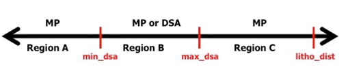
(Image courtesy Mentor Graphics)
But if that fab gives you one pitch, then that window is exceedingly small. Mr. Torres says that, with optimal chemical composition and guiding pattern, your pitch range will be on the order of ±5 nm. That’s not much. So for holes that don’t have the ideal spacing, you must turn to simple double-patterning. Just to be clear, you can do DSA and double-patterning together as a way to avoid triple- and quadruple-patterning.
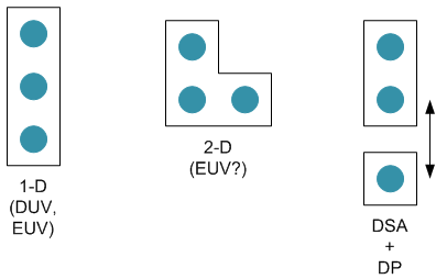
Having addressed the issue of pitch within the group, we come back to the question, “How many holes should we try to create at the same time, within the same group?” Right now, the rule is set to three. You can do more, but you can’t be confident that you’ll get good yield.
The second question is whether those three (or however many) should be in a line, or whether any old arrangement is allowed? This depends on your lithography. Today, the only option is deep-UV (DUV) exposure, so all the holes must be in a line – a 1-D restriction. If you’re using EUV, it’s possible to go 2-D (for instance, an L-shape). But less experimentation has been done with 2-D shapes, meaning the fab has less confidence – meaning that, for practical purposes, they will also likely be 1-D. It would take an “enlightened” engineer (to use Mr. Torres’ word) to successfully manage a more complex shape to yield well.
One side benefit of DSA concerns a bugaboo that’s been affecting standard lithography as dimensions get smaller: so-called line-edge roughness (LER) or a closely related concept, line-width roughness (LWR). There’s an interaction between resist sensitivity, LER, and feature resolution such that you get the classic, “Pick 2 out of 3” choice. You can’t optimize all three together.
That means that, in order to get less LER on a pattern using resist of a given sensitivity, you have to use more exposure power (an expensive commodity with EUV).
Well, here’s the good news. The smoothness of the outside surface of the cylinders isn’t determined by resist or exposure. It’s the guiding pattern, not the cylinder, that suffers from those. The cylinder’s roughness is determined by the granularity of the polymers (which is very small). So you can expose the guiding pattern with lower power (increasing litho throughput), making a guide with rougher edges, and the contacts will still come out clean.
The impact on tools and flow
The research team has assembled a flow for DSA-based designs, and it looks as follows:
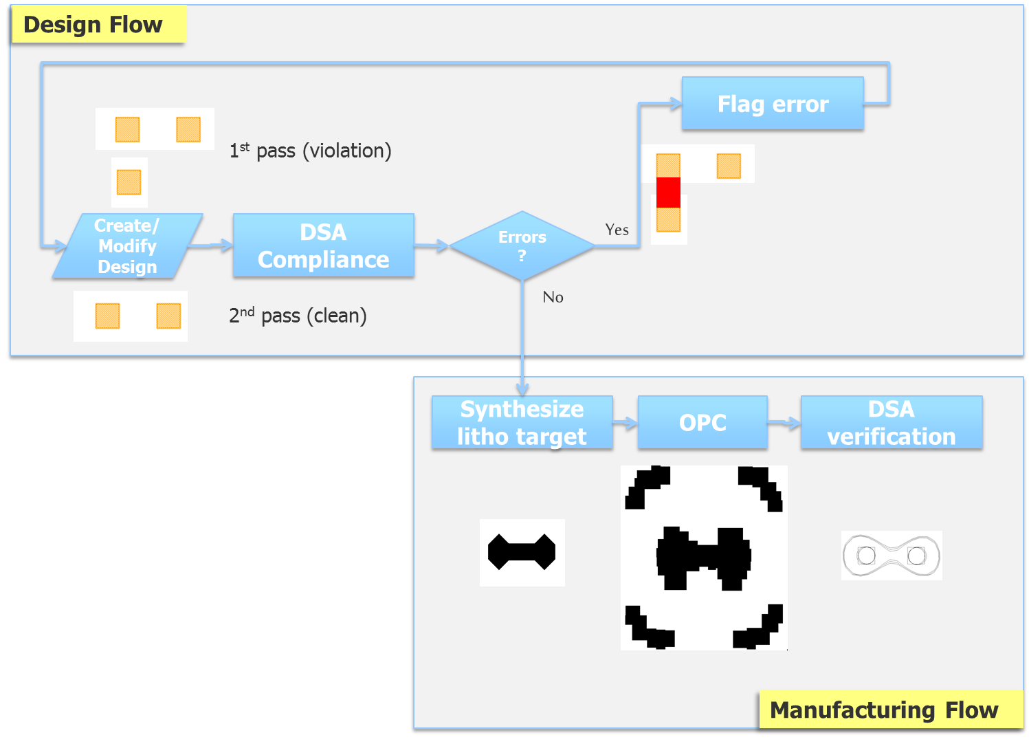
(Based on an image courtesy of Mentor Graphics)
There are two phases to this flow. The first is the design phase, and this is where interaction with the design and layout happens. As illustrated, let’s assume that, during the design, three contacts will be built in the L-shape above. This is determined by a tool that will automatically do the grouping.
Grouping gets complicated due to the 1-D and 3-hole rules. If you have five holes in a row, you have to use more than one group. That means multi-patterning (LE-LE, which becomes LDE-LDE, where “D” is the DSA step). And that means that the selection of which holes go into which groups has to take into account the spacing rules for the guide patterns and other effects. So it’s a complicated business, solved accurately by integer linear programming (ILP) techniques.
Problem is, those algorithms are very time-consuming – not suitable for a standard production flow. So a bunch of heuristics have been assembled that can be computed much more quickly, with their efficacy compared against ILP-based golden references. But it also means that, for any given design, it might not do a perfect job.
So the real-world flow will involve doing the grouping, testing for compliance, and then, hopefully, doing only a limited rip-and-reroute here and there to solve any violations. In the drawing above, the 2-D hole group is flagged as a violation (they have to be all in a row for DUV), and it looks like the spacing is too narrow with the bottom hole. So the error is marked for fixing (one of the holes will be removed from that group). The next test passes, and off we go to the manufacturing portion of the flow.
This is where a tool automatically synthesizes the guiding patterns for the hole groups using shape targets that, based on the prior experimentation, showed high tolerance of variation. Those shapes are then turned into the bizarre artifacts that optical proximity correction (OPC) creates, and then a final DSA verification is performed. These manufacturing steps are automated and (assuming the final check passes) would not involve the designer.
So there you go. DSA will first do holes for contacts and vias, and the number of holes you can do within a group will be limited to 3, all in a line. The flow has some extra DSA components, but most of the hard work will be done by tools.


What do you think about how DSA fits into the design flow?