


There are few semiconductor circuits as constant as the SRAM cell. Until now.
SRAM is important because it’s our fastest-performance memory tier – and it can take up a goodly chunk of your SoC area. But it’s an expensive beast (or else we’d use even more). For as long as I can recall, the basic reference circuit of the SRAM bit has stayed the same. It costs six transistors, arranged as a couple of back-to-back inverters with cross-coupling feedback to hold the state.

(Image source: Wikipedia)
There have been numerous tweaks and optimizations on this cell, but it has remained doggedly consistent for years. Now, however, for the first time I’ve seen, a proposal is on the table, announced at IEDM by a startup called Zeno, for a new SRAM cell. One that’s completely different from the one we know and love. And it requires only one (or two) transistors.
Seriously. Let’s not bother with in-between points of, oh, 5 or 3 transistors; naw, let’s get all quantum and jump all the way from 6 down to 1.
And, in case you’re wondering, it’s not a DRAM in disguise; it is truly static, with a non-destructive read and no refresh requirements.
Yup… I see those eyes narrowed in suspicion. If you could do it with one transistor, why are we just now finding out about it? What bizarre silicon production tricks and metamaterials are being brought to bear here?
Well, to hear Zeno tell it, there is nothing like that in their new cell; this is completely compatible with existing CMOS production. It requires one extra non-critical litho step and one extra implant. The CMOS compatibility is demonstrated by prototype chips that were built on a shuttle wafer, alongside other CMOS circuits.
So what the heck is going on here? They’re calling in Bi-SRAM because there’s an intrinsic bistable bipolar transistor in the structure they build. They take a basic MOSFET and then implant a buried N-well underneath. The buried N-well, the P-well, and the source/drain regions make up the NPN bipolar transistors.
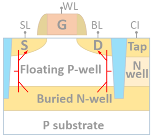
(Image components courtesy IEDM)
Schematically, I prefer to draw it as follows. (It’s upside down from how they show it, but it’s easier for me to picture with the bipolar transistor collector-side up.)
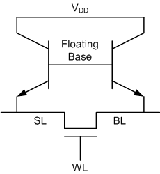
And, when it comes down to it, the idea is pretty simple, and it hinges on that floating base. You can think of it as a normally closed container for carriers. In one state, the base is filled with carriers. This turns the bipolar transistors on, opening a current path through the buried layer (which is connected to VDD – or should we call it VCC?) In the other state, the floating base is depleted of carriers, turning the bipolar devices off. You read the state through the MOSFET. If there’s lots of current, then some of it is coming through the collector.
That’s the underlying state mechanism, but you also need to be able to write that state – that is, either fill the floating base region with carriers or drain the carriers away. They do this by leveraging the capacitance between the FET gate and the floating P-well.
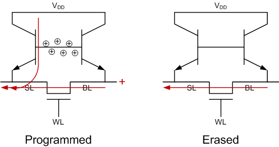
They didn’t go into detail on the algorithm, so this is my super-simplified summary of my understanding of their high-level description. They program one state by raising the word line and jerking up – er – raising with a carefully-controlled rise time – the word line. This couples to the floating base, punching the base up and turning on the bipolar transistors. This becomes a self-sustaining state based on carriers flowing in from the collector and now locked in the floating base.
To write the opposite state, you pull the source line down to a negative voltage to drain the carriers out of the base, snapping the bipolar transistors off. Yeah, you caught that, didn’t you… This does require a negative voltage pump. There’s roughly 6-8% more support circuitry for the cell, so you don’t get a full 5/6 size reduction net net. Only 4/5. Hope you can live with that.

The performance of the cell as shown is roughly comparable to that of a normal 6T cell; perhaps a bit slower. For high-performance applications, they have a higher-speed version that adds an extra select transistor. The 1T version exhibits leakage current through the channel on unselected cells, and this makes for a slower read. The select transistor cuts off the leakage, increasing the current’s dynamic range, which makes it easier – and faster – to read.
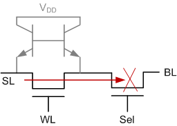
While this doubles the number of transistors, they can mitigate the effects through some clever layout; they refer to this as a 1.7T cell since it’s only 1.7 times the size of the basic 1T cell. But, as a bonus, it’s 40% faster than a 6T cell.
So, depending on which device you choose, it’s always smaller than a 6T (divide by 5 or 2.5), but may be slightly slower or 40% faster. Implemented in a 28-nm node, the 1T cell has area 0.025 µm2; the faster cell is 0.044 µm2.
Static power, meanwhile, drops by a factor of 5 (for either cell). Dynamic power is roughly the same as that of a 6T; maybe a little lower. For a battery-sipping IoT edge node, most of the time is spent sitting around snoozing – er – static, so one-fifth the power on a big (although now smaller) chunk of silicon could be exciting.
Now… I know what you’re thinking: maybe this works for the 28-nm node. But what about future nodes? Is there anything about this that might break a node or two down the road? And what about FinFET? They say that their approach scales with new nodes and that they can create a similar bistable mechanism for FinFETs. They see no obvious sunset clause.
A final question that I naively asked: is this only for embedded applications, or could it be used for stand-alone SRAMs as well?
And the answer there is, “Who still uses stand-alone SRAM?” OK, yeah, there is still a good business for a few players, and this technology could be put to use there. But that’s not the growing sector of the market in the way that embedded SRAM is. And so their focus will remain on the embedded side.
As you can well imagine, this is a licensing play, so, having taken the wraps off, these guys are now busily talking to potential licensees. Probably no surprise that this might turn some heads. If all works as promised, this could be one of those rare impulse functions acting on the market. You might be able to tell your grandkids one day that you were there when SRAMs went from six transistors to one… Pretty dramatic stuff.
More info:


What do you think of Zeno’s 1T SRAM cell?
Isn’t the real high volume use of static ram in the paging tables and caches of processors? Maybe the control memory for FPGA’s?
Curious if there are any SEU benefits over 6T designs.
If the essence is the charge in the base region then why this cell is better than the dynamic RAM cell is?
Or why 2 npn transistors are needed, but not a single one?
In my opinion, the gate terminal negative voltage forces some quasi current source, which feedes the bases of transistors. A positive gate voltage latches the 2-transistor network in some stable state with minimized base current of one of transistors.
Thank you for the comments.
With regards to SEU, we haven’t conducted SEU tests at this point. However, we expect SEU benefits over 6T-SRAM due to the smaller cross-section area for SEU.
With regards to DRAM comparison, the cell is static, so no refresh operation is needed. Read operation is also non-destructive.
The static behavior is governed by the npn bipolar formed by buried N-well, P-well, and source/drain regions. There are 2 bipolar since MOS has source and drain, but 1 is sufficient to achieve bi-stability.
We’ll update our website (www.zenosemi.com) with more details about the bi-stability mechanism. Please check back shortly.
-Yuniarto
Isn’t it rather 3T to be compared with the traditional 6T SRAM cell, looking at both schematics and area footprint?
In terms of functionality, you’re correct that it can be thought of as 3T. However, with regards to the area footprint, it is 1T (the cell size at 28 nm is 0.025um2, compared with 6T size of 0.127um2). The schematic cell drawing in this article includes a well tap, which is shared among many memory cells.
You are depending on the floating pwell to store the charges. Depending on the amount of charge is stored, it still could leak out through the gate as well as the SD and buried layer junctions. If the buried layer is powered up to VDD it could leak charges into the floating pwell to convert an unprogrammed cell into a program cell. We see this phenomenon in partially depleted Soi transistors. In essence this is a dynamic RAM equivalent but probably smaller footprint of 4f2 instead of the 6f2 of most drams.
Deep NWELL historically has more pipes (defects due to the higher implant energy) and that will exacerbate the leakage path into the floating pwell. It will be very dependent on anneal process while regular cmos is much less sensitive to defects of the buried layer.