


Four years ago, EDA in the Cloud was cool. Since then, it seems to have, well, cooled off. Until recently: it’s once more showing signs of heating up in an attempt to become cool again.
Cloud computing has always been problematic for EDA. Anything requiring the transfer of company jewels into unknown hands has too often been a deal breaker. The noise made by Synopsys and Cadence several years ago has noticeably subsided. OneSpin added a cloud capability, but only by promising not to send design information into the cloud – only abstracted proof requests.
But at this year’s DAC, two new cloud offerings appeared, and they’re handled in different ways. And, to varying degrees, they try to take into account the security challenges of the past. Both offerings target small companies that have a harder time affording full-up internal tool suites. They also hope for some medium- or large-company business when peak usage causes spill-over.
Am I Blue, Yes I’m Blue
The somewhat more straightforward offering comes from IBM. Yeah, bet you didn’t see that coming. Of course, if you’ve done an ASIC with IBM, then you’ve probably used their tools. If you haven’t, then you might not even know that they have their own tools.
They say that they tried to market their own tools in the ’90s, but it didn’t work out so well. Support, in particular, was problematic (presumably both for IBM and for users). So that largely disappeared. But a cloud model promises to be much easier to support.
The thing is, however, the tools themselves sound like rough-hewn workaday tools, without a shiny user interface to abstract the command line (for those who eschew the command line). So they teamed up with SiCAD, who has effectively put together a presentation layer for the tools. Users of the cloud offering will see the SiCAD layer via their browsers.
IBM is using their own SoftLayer cloud infrastructure to host the tools. Machines are single-tenant (where a tenant is a project) with a dedicated VLAN; communication is over a VPN. As a user, you’ll pay by the hour (costs vary by tool) and, if you want permanent storage, per GB per month. There’s no underlying cost if you don’t use the tools in a given month. Critically, designs can be revision-locked to ensure that tool revisions mid-project don’t upset design progress and metrics.
I see a couple of challenges for the current iteration of this offering. First is the fact that they’re not offering a full flow – yet. The starting lineup includes library characterization, SPICE, and logic verification. So, for instance, for SoC designers, that’s basically one tool – a simulator. Although they claim that the simulator runs 10-20 times faster than your typical incumbents – fast enough, they say, that some of their customers feel like they can get away without using emulation. That performance could be reason enough to attract some business.
And because the tools are different, they say that decisions to use them (or not) have to be made early in the project. This affects, in particular, companies that want to use the tools on an as-needed basis for extra capacity. Since they’re not offering the tools for non-cloud installation, then, by definition, such companies would be using one simulator in-house and then spilling onto a different one in the IBM cloud. That, in theory, shouldn’t matter (verification is verification, right? Right?); even if that works seamlessly, I’m not sure whether metrics folks will have any issue with comparing results of different tools.
Small companies, in the meantime, would need to buy their own in-house tools until IBM can fill out the flow. Which is a work in progress; they say they have 90% of the tools needed, but they’re adapting them to the cloud model. They are promising a full flow. (Timing unclear…)
By the way, in case you’re wondering what to call the IBM tools (other than just “the IBM tools”), it turns out that you should call them… the IBM tools. Apparently, IBM has a lengthy and laborious branding process that would take six months to complete. They didn’t want to wait for that.
Polished Chrome
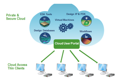
Meanwhile, Silicon Cloud is taking an entirely different approach. For security reasons, you won’t be able to launch your browser to get to your design in their cloud; you need a dedicated box with a “thin client” to get there.
Silicon Cloud has built their own private cloud facility, and they’ve outfitted it with carefully established user roles and permissions as well as lots of internal monitors intended to identify any odd activity. User behavior is tracked. The servers are multi-tenant, with containerization provided by the OS.
User interaction is possible only through a custom Chromebox designed by ASUS – a separate system that hosts a version of Google Chrome but exposes only the user interface that they’ve designed. You can’t go check your stock quotes through this box; you can do only what the Silicon Cloud user interface allows. The box has no other ports available – a feature intended to boost security.
The intent is that designs will be created and processed entirely in the cloud, minimizing the amount of design data upload and download. So most of the I/O to and from the cloud will simply be the user interface. And, in that case, the data coming down from the cloud is literally pixels, not design information (other than whatever might be on the screen at that moment).
They say they have four-factor authentication, although it feels more like four contributors to security:
- Standard two-factor authentication (a one-time password plus a per-use password)
- The Chromebox
- A trusted boot process
- VPN-only access
(Image courtesy Silicon Cloud)
That’s the security story – which is critical. Security aside, they are targeting full flows, starting with the reference flows at various foundries. It might be possible to craft a custom workflow, but they don’t expect small companies to want to do that. Small companies will be differentiating themselves not by some proprietary workflow that might give them an advantage, but by their specific product ideas.
They have a couple of business models: one for universities and one for commercial use. All the tool players participate in the university version, but Silicon Cloud is still working on agreements regarding who will participate in the commercial side of things. Their intent was to announce the flow(s) in July (as of this writing, I haven’t seen that announcement yet) with availability in September.
Their focus will be on semiconductor and sensor design. That latter one clearly indicates the need for mechanical tools as well as electrical ones, so that could be another differentiator for them. Billing will be on a per-use basis, both for software and hardware used.
What both of these offerings indicate is the higher level of investment required to establish a credible cloud-only flow. And, frankly, we won’t know whether their greater commitment pays off until we see whether they’re able to attract significant levels of business. We’ll need to come back in a year or so to see what the results have been.
Update: In my original posting, I had noted tha the Silicon Cloud website appeared to be down or compromised somehow. Shortly after posting, I checked again, and it appears to be back up.
More info:
IBM/SiCAD offering (via SiCAD)


Do these new cloud-based EDA offerings adequately address security, to the point where you could use them?
At least working with IBM and Globalfoundaries It’s likely your IP will stay in the US. Doesn’t mean that Asian IP theft rings can not insert/purchase Globalfoundaries employees. At least with the majority of the company inside the US, we have US laws and jurisdiction to fight back against theft.
With Silicon Cloud it’s unclear the physical and personnel security controls are likely to be as effective against organized IP theft rings. And it’s likely your data will end up outside the US, and you will lack effective legal recourse off shore.
Still seems if your product and IP is worth more than the tools, buy the tools.
Hi,
Thanks for your interest in Silicon Cloud and its design collaboration platform. I would encourage you to visit our website http://www.siliconcloudinternational.com/ to find out more about our company. You may also download technical white papers to learn more about the security and high performance of our platform.
Below is an abridged version of the white paper:
Silicon Cloud is committed to building private and secure cloud computing centers worldwide. Our secure cloud enables our partners in the IoT & IC design ecosystem to reap the benefits of cloud computing, and to reach a new level of collaboration both within and across organizations. This is not just simply putting EDA software into a public cloud like Amazon AWS. Silicon Cloud designs the entire system from the ground up: the cloud hardware infrastructure, cloud middleware, semiconductor design workflows, and security features in the system. With this, Silicon Cloud is able to provide new features and a user experience never before seen in the IC design ecosystem.
The salient features are:
1. End-point access via Silicon Cloud issued thin client is strictly controlled with a 4-factor authentication system.
2. All data are encrypted and stored securely in the cloud database.
3. Effective monitoring and policy enforcement in the cloud, ensuring rules are strictly followed.
4. In addition, there are other benefits and features offered by Silicon Cloud’s system (e.g. software pay-per-use metering, IP tracking, and audit trace) which are not readily available in today’s IT systems.
Silicon Cloud’s extremely secure environment, as well as its high performance will certainly enhance collaboration both within and across organizations, leading to shorter development time, and improved innovation in the semiconductor ecosystem.
The “Silicon Cloud’s extremely secure environment” certainly has easy security attacks with an inside job or an anonymous remote “root kit” attack that reaches the operating system command line with privileges.
If the Silicon Cloud tools can access “clear text” unencrypted data, as is required to function, then your design can be easily copied with the right attack. This is clearly the inside/remote attack that IP theft rings will seek.
It really doesn’t matter what the authentication and high security encryption system is, if the system has a back door to log customer keys and certificates, or a back door to side copy clear text files and designs while they are being processed.
Processing your data outside your own data center, means that data WILL ALWAYS BE EASILY COPIED by rogue staff intending to sell it to the highest bidder. AKA a Snowden style attack that caught the NSA with their pants down, which is exactly the attack IP theft rings will use.
The same is true with your own staff … at least that you have direct control over, and can manage risks.
Silicon Cloud will need to provide a meaningful disclosure bond with a value including lost future earning on the product to mitigate REAL IP theft ring realities. And hopefully that bond house, will tighten the screws on Silicon Cloud enough, that personnel are very carefully vetted, and physical security controls are exceptionally well monitored.