

So you’re working on a big die, eh? Maybe a huge imaging die – sized to capture a wide field with high resolution? Yeah… die manufacturing yield isn’t so great, eh? What to do?
When you’re on an unfriendly part of the yield curve, yield drops non-linearly with die size, meaning that 4 dice that are ¼ the size of one big die will yield more than four times better, combined, than the one big die. (If both big and small dice are already yielding 99%, then four small dice won’t yield better than 100%…)
So if your monster die isn’t yielding so well, it would be nice to fashion it out of smaller dice. But, traditionally, that’s not so easy: you have to lay them out on a substrate (perhaps an interposer with a redistribution layer (RDL)) and use wirebonding (or flip-chip with bumps, leveraging the RDL) to hook everything up. The signals going through those wirebonds (or the RDL) are not going to perform the same way that the on-chip connections would, and you’ll have a fair bit of space between the dice, which will create a seam or gap in the image –like the effect that monitor bezels have on a wall-of-monitors.
So… maybe you could fake it with interpolation algorithms; maybe not.
Much of the attention around cobbling multiple dice together inside a single package has been about going vertical – the 3D solution made possible by through-silicon vias (TSVs). While there is clearly going to be a home for that technology, it’s not without its challenges.
Many of those challenges have to do with heat. As in, how to get rid of it, and – more subtle – how to deal with multiple dice made from different materials with differing coefficients of thermal expansion (CTEs).
Then again, those completely miss the point for the array application: stacking the four dice simply doesn’t make sense. In other words, there are a number of situations where 3D TSV technology may not be ideal (even without considering cost).
Indiana Integrated Circuits (IIC) believes they have a viable alternative to vertical packaging: it’s a better way to stay horizontal by literally soldering the component dice together into what can function, mechanically, as a single heterogeneous die. They call it “quilt packaging.”
It doesn’t have to compete with TSVs – they can be combined to provide complex mechanical arrangements of dice in ways that could yield extraordinarily unusual shapes. Whether those extreme shapes have commercial value remains to be seen, but they’re merely an extrapolation of the technology – they’re not the reason for it. More on that in a minute…
The fundamental idea here is much like the bump-and-reflow way of handling vertical stacking. The difference is that, instead of creating pads with bumps and deep vertical vias, you create “nodules” on the die edges that will mate together. These nodules are ultimately interconnected and reflowed, creating an unbroken connection between the dice. Signal quality rivals on-chip signaling, boosting performance. The mechanical strength is high enough that you can handle the assembled unit as if it were a single die.
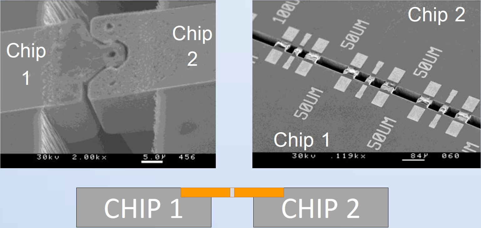
Image courtesy Indiana Integrated Circuits
The nodules can be pretty much any shape you want. You see one on the left above that “interlocks”; that’s merely an option.
But it gets more surprising than this: not only can you make electrical connections across dice, you can make optical connections as well. You can control the spacing between dice to minimize the gap (IIC considers less than 1 µm to be fully abutted), or you can create a larger gap to control how optical modes transfer.
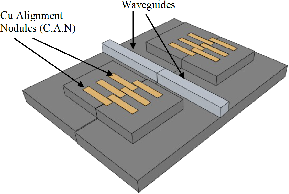
Image courtesy S. Howard & S. Hoffman, University of Notre Dame
You can even change materials when coming across – using a “funnel” shape (much as we saw in our coverage of photonics basics last year) can help the transition.
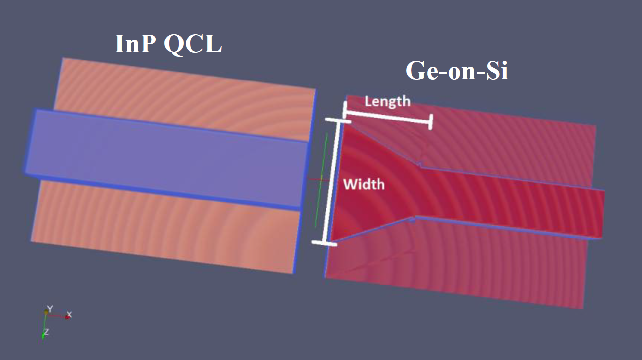
Image courtesy S. Howard & S. Hoffman, University of Notre Dame
The fabrication is similar to a via-middle process, building up the metal on the edges. And once the die is passivated, then the passivation is etched for the nodules on the side, much like bond pads are etched to open them up. They do require at least two extra lithography steps: one to pattern the nodule and one to define the dicing street, plus plating and chemical-mechanical polishing (CMP) steps.
It also requires etch singulation. Running the wafer through a bandsaw wouldn’t be great for the nodules… We looked at Plasma-Therm’s proposals for etch singulation last year; the ability to be more creative with how dice are arranged and shaped helps with the quilt packaging as well. According to IIC, acceptance of etch dicing is growing, so this should recede as a concern.
As to how effectively you can assemble a whole out of parts, let’s start with the simple example above: building a large image array out of multiple smaller arrays. You may still ask the question, “What about the seam between the dice? Does that interrupt the image?”
Well, according to IIC, you can get the dice so close together that you don’t have to interrupt the steady flow of rows and columns – there will be no seams. If that’s the case, then you can build a continuous big array out of smaller components.
That’s a simple planar example, but you can also go 3D with these – in a different way from what you might have expected with TSVs. For example, you can take a die and fashion it into a backplane. You etch rows of plated holes in the back or front side and then plug other dice side-on into those holes. In other words, each of those plugged-in dice looks like a blade, with the blade’s nodules connecting through those holes in the backplane die.
Or you can create a cube, designing the nodules to dovetail like finely crafted cabinetry. You can even make a bucky-ball geodesic dome shape – creating approximations of curves if large enough. Such arrangements have particularly good mechanical stability.
There could still be a question, however, regarding thermal mismatch here as well. Particularly because IIC says that this works nicely for interconnecting dice made with different materials – raising the possibility of CTE mismatches again. We’ve seen that this is a challenge for stacking dice, but what about attaching dice side-to-side?
In theory, if the dice expand at different rates, you’ll get stresses at or near the nodules. Does this cause any problems? I checked with IIC about this, and their practical answer is that they’ve never seen a problem with it – even though mixing materials is one of their strengths. One aspect that helps is that, on a heat-intensive planar application, all of the bonded-together dice are on the same heat sink, which should help to reduce the amount of expansion.
Even so, empirically, they’ve never seen a failure of this sort. They continue to test, but so far so good.
It bears noting, by the way, that they’ve worked with almost all of the obvious wafer materials – except for sapphire and diamond. They’re very hard to etch, so they haven’t tackled them. (Yet, anyway…)
The next big question is, “What’s the future for high-volume commercialization of this technology?” There’s some chicken-and-egg going now: fabs want to integrate only technologies that designers are committed to using. And designers will commit to using only technologies that are available in the fab. IIC is trying to break that impasse. It’s also not set in stone where this process would happen: it could be in the foundry or at the offshore assembly and test (OSAT) contractor.
From a cost standpoint, these days it’s a project-by-project calculation. Pending high-volume development, they’ll continue on with specialized projects (defense, for example).
But they stress that, from a technological standpoint, “there are no showstoppers.” It’s now largely a business and partnership challenge.
More info:
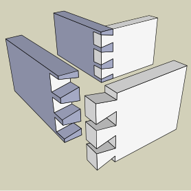
Cover image credit: “Joinery-throughdovetail” by Joinery-throughdovetail.gif: SilentCSVG conversion: Duncan Tate (talk) – Joinery-throughdovetail.gif. Licensed under CC BY-SA 3.0 via Wikimedia Commons – http://commons.wikimedia.org/wiki/File:Joinery-throughdovetail.svg#mediaviewer/File:Joinery-throughdovetail.svg


What do you think of this quilt packaging approach to interconnecting multiple dice?