

[Editor’s note: this is the fifth in a series of articles derived from a session at this year’s ISSCC that focused on sensors and energy harvesting. The prior article dealt with a high-voltage current sensor. For more details, you are referred to the ISSCC proceedings.]
Most of us don’t know what it’s like not to be able to see clearly, even if with the aid of eyewear. Now, you might say that, for the great majority of us, we actually experience a certain blindness everyday: we can’t see an imminent apocalypse the way a select few can. (OK, perhaps fewer than was thought a week ago.) But that’s not the same thing.
The world operates on the principle that only those with a special direct line to a higher power get the end-of-days news before it’s printed. The rest of us aren’t expected to be able to work that way, so we get a break. Not so for the conventionally-blind: the world is overwhelmingly set up to assume visual processing of our surroundings, so those without access to vision are at a distinct disadvantage.
Of course, where medicine can heal blindness, the problem is solved. Where that doesn’t work, technology can help out, depending on the cause of the issue. Vision counts on the eye to capture and focus an image, a neural connection to relay that information to the brain, and visual brainware to process it and create the experience of seeing. Break any of those and you will be blind.
If the problem lies in the eye, perhaps with faulty rods and cones, then, the thinking goes, we can replace the natural, misbehaving light sensors with artificial sensors, delivering the alternative image to the optic nerve for the brain to interpret. You could strap an external camera pretty much anywhere, as long as you could somehow patch it to the brain, but the most natural place – both functionally and aesthetically – would be inside the eyeball itself. Hence the so-called retinal implant.
But circuits need power, and you’ve got to have some way of getting juice to the sensor – and that’s much harder if the sensor is buried deep inside vitreous humor. What if the very light being sensed could also be harvested to power the sensor?
That’s the fundamental idea behind a project taken on by Suat Ay at the University of Idaho. He noted that the photodiode that senses light is more or less the same as the photodiode that generates power in a solar cell. The configuration is slightly different, but circuitry can take care of that.
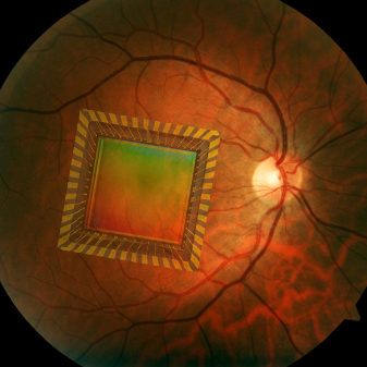
To plumb this project, let’s start by looking at the sensing side. He used a 3T active pixel sensor (APS) for imaging. Also known simply as a CMOS sensor, an APS sensor is inexpensive and can operate on lower power as compared to the older charge-coupled device (CCD) technology, although apparently at the expense of some fidelity.
Operation is simple. A photodiode is reverse biased, and the cathode – the “pointy end” (I always forget which is which) – is normally a floating node. A reset pass transistor precharges the node; left on its own after the reset path is closed, the node drives a source-follower transistor that tracks the node voltage (high impedance because it’s MOS). As photons strike the photodiode, electrons are generated, pulling the node voltage down. The resulting sensed voltage determines the image for that pixel, and an array of these gives a complete image.
The power-generating diode operates upside down, with the anode connected to the harvested energy line. As photons hit it, electrons go the other way, creating a potential across the diode.
In this chip, operation was divided into two distinct modes: a sensing mode and an energy-harvesting mode. One extra transistor was added to short the APS diode when in energy-harvesting mode. In sensing mode, the harvested power bus (at the anode of the power-generating diode) is grounded, so now both diodes act as sensors, increasing sensitivity.
Being able to manage low power becomes even more critical when the chip has to be self-sufficient: it’s not just a battery-life issue; it’s a “will the dang thing work?” issue. So in order for various critical circuits to operate at a very low voltage, he used supply-boosting technology (SBT). This is a simple circuit that doubles the actual supply voltage locally where needed.
Like any booster, it relies on charge pumping, and it’s typically fed by a clock to keep the boosted node stable. In a few instances in this design, it’s driven by a signal – like reset, for example – so it’s edge-sensitive. The edge event creates a window within which the relevant circuit gets a voltage boost.
So how did it work? Did the chip power itself?
Well… it actually wasn’t set up to do that this go-round. It seems more of a proof of concept, since switching between sensing and harvesting modes is done manually off-chip. And the power harvested doesn’t drive the internal circuit; it drives either a charge pump or a simple direct-measurement node, both off-chip. This allowed the basic circuit to be tested, along with measurement of both the amount of power generated by the harvester and the amount of power consumed by the sensor.
So then the question is, how does the balance sheet look?
Well, conceptually, everything worked, but this particular project demonstrated deficit spending. The harvested power, of course, depends on how much light is available. This is measured in lux units: luminance per area, equivalent to lumens/m2. At 60,000 lux, typical for sunny daylight, they generated 3.35 µW. Normal daylight is more like 20,000 lux, yielding 2.1 µW, and an overcast sky takes things down to 1000 lux and 1.0 µW.
In imaging mode, with a 1.2-V supply and at a 7.4-frame/s rate, the circuit consumed 14.25 µW. More than is harvested, but, then again, the harvested power could certainly keep a battery going longer; something is better than nothing.
But, as a proof of concept, the basic circuits work, and the imager figures of merit compare very favorably against prior work (and the prior work was on more “aggressive” 0.35-µm technology, as compared to 0.5 µm for this project). So perhaps we’ll see a fully self-sufficient sequel at an upcoming show.
(Note: you can find the next article in the series here.)

